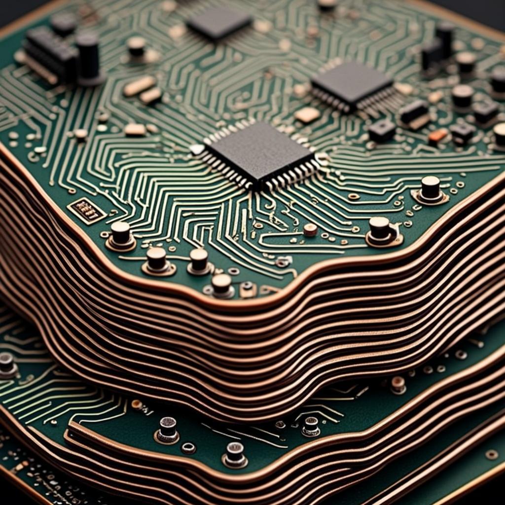
Designing rigid-flex PCBs combines the challenges of both rigid and flexible circuit design. Here are some common mistakes made in the design of rigid-flex PCB assemblies and how to avoid them:
Mistake: Designers often apply rigid PCB design principles to rigid-flex designs, failing to account for the unique properties of flexible sections.
Solution: Understand the specific requirements of rigid-flex PCBs. Flexible sections need different design rules, such as avoiding sharp corners and ensuring smooth transitions between rigid and flexible areas. Use design tools that support rigid-flex PCB design to simulate and validate your designs.
Mistake: Incorrect via pad sizes can lead to manufacturing issues and reliability problems.
Solution: Ensure that via pad sizes are accurately specified for the drill sizes used. Consult with your fabricator to confirm the appropriate sizes and tolerances.
Mistake: Placing plated through holes (PTHs) too close to the transition from rigid to flexible circuitry can cause mechanical stress and potential failure.
Solution: Maintain a safe distance between PTHs and the transition areas. Follow guidelines for minimum spacing to reduce stress and improve reliability.
Mistake: Using too much copper on flexible layers can reduce flexibility and increase the risk of cracking.
Solution: Optimize the amount of copper used on flexible layers. Use cross-hatched patterns instead of solid fills to maintain flexibility while providing necessary electrical performance.
Mistake: Solid copper layers in flexible sections can lead to reduced flexibility and increased risk of delamination.
Solution: Use cross-hatched copper patterns in flexible areas to enhance flexibility and reduce the risk of delamination.
Mistake: Incorrect amounts of adhesive in the layer stackup can lead to delamination and mechanical failure.
Solution: Follow precise guidelines for adhesive application in the layer stackup. Work closely with your fabricator to ensure the correct amounts are used.
Mistake: Failing to define the bend radius can result in excessive stress on the flexible sections, leading to cracking and failure.
Solution: Clearly define the bend radius in your design documentation. Ensure that the bend radius is appropriate for the materials and thicknesses used in the flexible sections.
Mistake: Sharp angles in trace routing, especially in bend regions, can cause traces to crack or break.
Solution: Use smooth, curved traces instead of sharp angles. Avoid routing traces through bend areas whenever possible.
Mistake: Placing vias in areas that experience high stress, such as bend regions or near stiffeners, can lead to mechanical failure.
Solution: Avoid placing vias in high-stress areas. If vias are necessary, reinforce them with additional support or use alternative routing strategies.
Mistake: Failing to properly capture Surface Mount Technology (SMT) and unsupported pads can lead to pad lifting during assembly.
Solution: Ensure that all SMT and unsupported pads are adequately supported. Use anchoring spurs and pad fillets to increase the strength of the pad-to-trace interface.
By understanding and addressing these common mistakes, designers can improve the reliability and performance of rigid-flex PCB assemblies. Collaborating closely with fabricators and using specialized design tools can help avoid these pitfalls and ensure successful rigid-flex PCB designs.