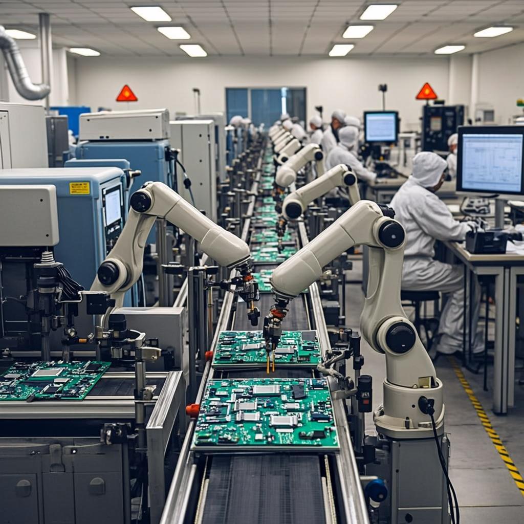
Have you ever thought about the small green boards you see inside your favorite gadgets? The boards are known as printed circuit boards (PCBs), which connect and power all the intricate components that enable your devices to function. Before a PCB is incorporated into any of your devices, it undergoes various stages of prototyping. Let’s take a closer look at the key steps in creating a printed circuit board prototype, starting from the concept to the final testing phase.
A rough version of a project is often referred to as a prototype, and the same applies to a PCB prototype. As with any project, a first draft is rarely the final version and typically requires revisions. Similarly, a PCB prototype serves as a revision and an opportunity for designers and engineers to evaluate their prototypes before mass production, identify potential issues, and fine-tune the design. This minimizes unnecessary expenses during production and future losses due to faulty designs.
For a successful project, a detailed and organized plan is crucial, and this holds for PCBs as well. To ensure the intended goals are successfully achieved, defining the functions of the PCB is a step in any project.
Identifying potential questions is very helpful. These include: What does the board need to control? How large should it be? What components will it require?
Examining competing products is also helpful. Determine what features are effective and where there is room for improvement. Thoughtful planning paves the way for the best PCB prototype.
We’re going to get technical now, but don’t stress out. We will keep things really easy. PCB design is somewhat akin to blueprinting your board.
Tip: No matter how simple it is, check and recheck. Small details matter a great deal, especially how they will impact things downstream.
The sequence to refine is the schematic, ready, and defining.