People first, Strict management, Treat cusomter with sincerity, Survive on high quality, Promote through technology, Show strength with distinctive features,Improve efficiency with speed.
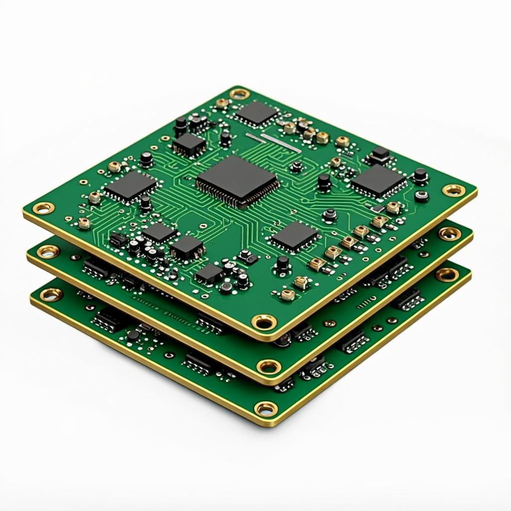
Board thickness:rn≥2.0mm G/F thickness:≤1.6mm±0.1mm G/F tolerance:±0.05mm Layer count:≤44 layers
Structure:Partially / fully embedded Min coin size:2*2(mm) Min coin thickness:0.5mm Flatness between coin and base material:≤0.075mm
Material:AIN Embedded Ceramic size:20*20(mm) Professional technical support for thermal management:
Max board thickness:6.0mm Max aspect ratio:25:1 Max gold thickness:80 u'' Warpage:≤4‰
Address: No.389 Shetang road, Economic and Technological Development Zone, Changsha, China.
TEL: 0731-82786288-6818
Email: pcb@frankenthalerfoundation.org
Copyright 2021 © MULTILAYER PCB TECHNOLOGY CO., LTD ALL Rights Reserved