Our 4-layer and 6-layer PCBs engineered for industrial control systems are built to withstand the harsh operational conditions of factory floors—far exceeding generic manufacturing benchmarks. The 4-layer PCB leverages high-Tg FR-4 material with a glass transition temperature of ≥170°C, enabling stable performance across a -40°C to 85°C temperature range. Equipped with 3/3mil line width and spacing, plus 0.2mm via diameters, this board supports 24V industrial power inputs while incorporating dedicated anti-interference shielding between signal and power layers. For complex programmable logic controllers (PLCs), the 6-layer variant adds an independent ground plane, cutting electromagnetic interference (EMI) by 30% compared to 4-layer designs. It integrates 0.15mm blind vias to eliminate signal crosstalk from through-holes, with full compliance to IEC 61010 industrial safety standards for hazardous electrical equipment.
Our 8-layer and 12-layer PCBs designed for automotive battery management systems (BMS) are fully optimized to meet AEC-Q200 automotive electronics qualification standards, with bespoke thermal and electrical enhancements. The 8-layer PCB adopts a symmetric stackup structure (signal-ground-power-ground-signal) to minimize warpage to ≤0.5%—a 50% improvement over the industry average of 1.0%—during prolonged operation in high-temperature engine bays. Its 2/2mil line width and spacing accommodate high-density cell monitoring circuits for EV battery packs. The 12-layer version integrates two dedicated thermal dissipation planes and 3mm×3mm copper coin reinforcement for 100A high-current pathways, a critical feature for BMS supporting 100kWh+ battery configurations. Every unit is backed by a 1000-hour thermal cycling reliability guarantee, ensuring durability in extreme automotive environments.
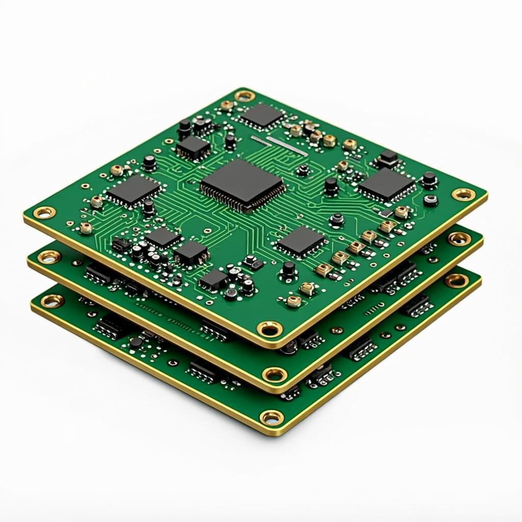
As a specialized manufacturer of 10-layer PCBs, our custom stackup design service addresses the core challenge of misaligned layer functionality in high-complexity electronic devices. For aerospace navigation systems, we engineer 12-layer PCBs with a symmetric “RF-signal-ground-power-ground-signal-RF” stackup, delivering ±2% impedance control at 50Ω for 24GHz satellite communication signals. The design combines Rogers 4350B material for RF layers (to ensure high-frequency performance) and high-Tg FR-4 for power layers (to optimize cost-efficiency). For high-performance industrial servers, the 10-layer PCB uses an asymmetric “signal-power-ground-signal” stackup to support 10Gbps data transmission speeds. It incorporates precision back-drilling to eliminate stub noise in high-speed signal channels, preventing signal degradation in bandwidth-intensive applications.
Our 16-layer PCB—our highest-tier customized layer option—undergoes a proprietary 7-step reliability testing regimen, far surpassing basic industry inspection standards for high-complexity projects:
Every 16-layer PCB shipment includes a comprehensive compliance report, fully suitable for regulatory submissions in aerospace and defense sectors.
A leading industrial robot original equipment manufacturer (OEM) partnered with us to resolve critical dust-proof and anti-static flaws in their standard 6-layer control board, a problem their previous supplier failed to address. Our engineering team delivered three key custom modifications to the 6-layer PCB:
The modified board passed 5000-hour factory dust chamber testing with zero performance degradation, cutting equipment downtime by 40% compared to the original design. Notably, the entire project was completed and delivered within 15 days—30% faster than standard industry lead times.
A mid-range electric vehicle manufacturer required a custom 12-layer PCB for their next-generation BMS, as off-the-shelf boards could not fit their compact battery pack enclosure or support 100A current demands. We engineered three targeted optimizations for the 12-layer PCB:
The custom PCB fit the enclosure perfectly, passed all AEC-Q200 qualification tests, and reduced the client’s BMS costs by 12% compared to importing equivalent foreign-manufactured 12-layer PCBs.
These are network equipments to connect LAN with LAN or LAN with WAN. Router is an equipment playing the role of a guide to ensure appropriate communication among several networks by mainly taking charge of outside communication networks. Unlike Router, Switch is an equipment taking charge of the independent network where input speed is guaranteed without delay even when communication volumes are increased by guaranteeing the rated communication capacity despite crowding of several packets in the packet transmission path.
It is a circuit board playing the role of a connector between Router and Switch, which is mounted with a type of inserting slots in the actual large backplane by several routers/switches and other devices to create a path to transfer data between equipments.
Backplanes or “back panels” are typically higher layer count than standard PCB’s, often 20 to 40 layers or more. They are large and thick, with rows of press-fit holes for high speed connectors. The connectors allow daughter-cards or line-cards to be plugged in and swapped out easily. Backplanes may be passive or active, with passive ones lacking on-board processing and memory devices. In some cases, line-cards may plug in from both sides, in which case the boards are called Midplanes.
The applications for backplanes push these boards to extremely high speeds (>100 GHz). The reliability of data transmission is critical to ensure 0 packet loss. Signal integrity (SI) therefore becomes very critical in backplane systems.
The base materials used in backplanes are usually very low loss, and may also use low Dk glass and HVLP copper foils. Rotation of the image on the production panel or use of zig-zag routing may also be used to minimize weave effect and skew.
Backdrill is utilized to remove the unused portion of PTH’s (stubs) which cause signal reflection and degrade SI. Our state-of-the-art backdrill systems have panel mapping capability to ensure depth consistency and repeatability.
Benchuang can perform backdrill from both sides to various depths. Blind and buried vias may also be used to minimize the length of the barrels to improve SI.
Benchuang Electronics provides quick turn and production ba