Due to the increasing density of chip packaging, the interconnections have also become more compact. This brings a significant issue: single layer PCBs or double layer PCBs are no longer sufficient, leading to the adoption of multilayer PCBs. A multilayer PCB is a circuit board made by stacking two or more layers of circuits together, with reliable pre-defined interconnections between them.To better understand the necessity and complexity of multilayer PCBs (MPCBs), it is essential to first analyze the foundational limitations of simpler structures and the advanced engineering principles required to overcome them.
The rapid advancement in semiconductor technology, particularly the shift toward high-I/O count components utilizing Ball Grid Array (BGA) and Fine-Pitch BGA (FBGA) packaging, has made the use of single- and double-layer PCBs obsolete for almost all high-performance designs. The fundamental limitation of 2-layer PCBs (DLPs) is their inability to provide continuous, solid reference planes (Ground and Power) while simultaneously accommodating high routing density. In a DLP, traces must constantly jump between the two outer layers using through-hole vias, severely fragmenting the necessary reference return paths. This fragmentation introduces significant signal integrity (SI) issues, including increased crosstalk, substantial electromagnetic interference (EMI), and generally poor electromagnetic compatibility (EMC).
Modern semiconductor packaging, specifically high-I/O Ball Grid Array (BGA) components, often require extreme routing density, with pitch dimensions routinely less than 0.5mm. Routing the escape patterns beneath these components demands a high density of vertical interconnections that cannot be achieved efficiently using only simple through-holes.MPCBs provide the structural framework needed to transition routing from a planar (2D) approach to a stacked (3D) engineering solution.
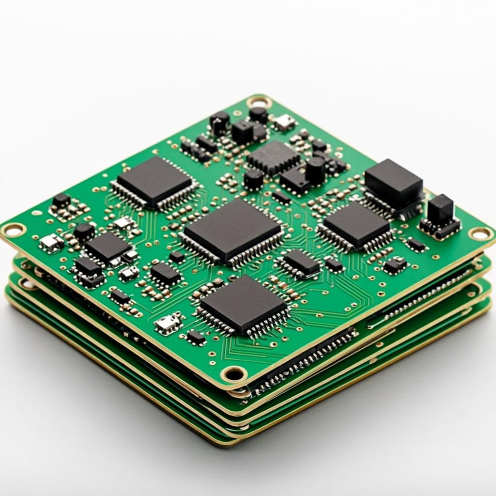
A multilayer PCB is a circuit board made by stacking two or more layers of circuits together, with reliable pre-defined interconnections between them. Crucially, an MPCB is a controlled stackup of conductive layers (copper foil) separated by prepreg (B-stage resin) and cores (C-stage laminate) that are laminated together under intense heat and pressure to form a solid, monolithic structure. The layers are typically designated for specific functions: Signal (S), Ground (GND), and Power (PWR), allowing for intentional, high-performance electrical routing.
The foundation of robust MPCB design begins at the 4-layer configuration. The four-layer structure (typically Signal, Ground, Power, Signal) is the minimum required to establish the necessary continuous reference planes for controlled impedance routing. This architecture immediately addresses fundamental SI concerns by dedicating two interior layers to solid, low-inductance return paths. Without these solid reference layers, high-speed signals cannot propagate reliably because the electromagnetic field of the signal trace needs a constant, adjacent return path to minimize loop inductance and prevent impedance discontinuities.
As design requirements exceed the capacity of a four-layer board, layer counts escalate significantly. Applications in complex computation, high-speed networking, and large data center infrastructure often necessitate extremely complex stackups.
High-end server motherboards and telecom backplanes routinely require 8, 12, 16, or more layers, pushing fabrication complexity to its limit. A fabricator's ability to handle these complex structures is a direct indication of their experience and expertise. For instance, NextPCB officially supports up to 32+ Maximum Layers, a specification that demonstrates top-tier capability in managing extreme stackup complexity, including high layer count sequential lamination, monumental thermal management, and achieving perfect layer registration across numerous manufacturing cycles.
The technical infrastructure required to successfully manufacture 32-layer boards is a strong signal of Authoritativeness within the high-reliability manufacturing sector, as these boards are generally utilized in mission-critical applications such as defense systems or central networking hubs.
The longevity and performance of a multilayer PCB are fundamentally determined by the base materials used. Mismatched or improperly specified materials are the leading cause of field failures, thermal fatigue, and signal degradation.
The selection of base materials (laminates) is the most critical decision impacting both electrical performance and mechanical reliability. The industry relies on standardized frameworks to ensure quality and compliance. IPC-4101 provides the definitive specification for rigid and multilayer PCB base substrates, ensuring that cores and prepregs meet standardized parameters for quality, thermal stability, and electrical performance.
By utilizing IPC classification numbers, designers can communicate precise and unambiguous requirements to manufacturers, aligning material characteristics—such as thickness uniformity, resin flow, and thermal expansion—with the final application needs.
Tg defines the temperature ceiling for the material's structural integrity. It is the point at which the polymer matrix transitions from a rigid, glassy state to a soft, rubbery state. Operating a PCB above its Tg leads to dimensional instability, which compromises the integrity of plated through-holes (PTHs) and can result in delamination.
For high-power industrial, automotive, or aerospace applications where internal operating temperatures are elevated, materials with a Tg above 170°C (e.g., 170°C – 180°C) are mandatory to prevent delamination and PTH failure during prolonged use. Standard FR-4 typically has a Tg around 130°C. The capacity to procure and process higher performance materials is a measure of fabricator capability. The ability of NextPCB to support high Tg materials up to 170°C – 180°C demonstrates capability for high-reliability manufacturing required in rigorous environments.
Td is the temperature at which the material chemically decomposes. This measure is crucial for determining safe assembly and rework temperatures. If the board is subjected to temperatures exceeding its Td during assembly (e.g., reflow soldering), the laminate permanently degrades, resulting in catastrophic failure.
For high-speed digital and RF designs, electrical properties supersede thermal or mechanical ones. The dielectric constant and dissipation factor dictate how fast signals travel and how much energy is lost.
The Dielectric Constant (Dk or ε r) directly influences the speed of signal propagation and the characteristic impedance (Z 0). Signal velocity is inversely proportional to the square root of Dk. For high-frequency applications (typically above 1 GHz), lower Dk values (e.g., 3.0 to 3.5) are necessary to minimize signal delay and maintain stable impedance. Higher Dk materials slow the signal and introduce more latency.
The Dissipation Factor (Df) represents energy lost as heat, which translates directly to signal attenuation. This loss is particularly problematic at high frequencies. Low Df materials are essential for high-speed digital and RF applications where signal loss (insertion loss) must be minimized. For cutting-edge applications, such as 5G infrastructure, materials with Df values as low as 0.0015 are often specified to ensure minimal energy attenuation and high signal quality.
High-speed and RF laminates, such as Megtron 6 or RO4350B, which exhibit very low Dk and Df, fall under the specific guidelines of IPC-4103. This designation signals their suitability for applications demanding precise electrical characteristics at extreme frequencies. The use of specialized materials under IPC-4103 confirms that a design is constrained by electrical physics rather than mere density.
The Coefficient of Thermal Expansion (CTE) measures how much a material expands when heated. High CTE, particularly in the Z-axis (thickness), subjects the plated copper barrels of vias to enormous stress during thermal cycling (e.g., soldering or operation). Excessive Z-axis expansion can lead directly to barrel cracking and connectivity failures.
IPC-4101 defines CTE limits to match materials with components and reduce stress. In a complex MPCB stackup (8 layers & 8+ layers), every layer adds thermal stress. Using low Z-CTE materials, often correlated with high-Tg properties (e.g., FR-4 4101/26, with Z-CTE of 70–90 ppm/°C), minimizes the expansion differential between the laminate and the copper plating, directly improving the long-term reliability of internal interconnections, which is paramount for long-term Trustworthiness in technical applications.
Layer separation, known as delamination, is a primary mechanical failure mode caused by poor bonding or severe thermal stress. IPC-4101 explicitly specifies prepreg resin content and flow properties to ensure robust adhesion during the lamination process.
The following table summarizes the material specifications critical for MPCB design:
The cost of moving from commodity FR-4 to specialized materials (IPC-4103 certified) represents the steepest cost trade-off in MPCB manufacturing. This is evident in pricing models where even a moderate increase in thermal requirement, such as specifying Tg from 130°C to 170°C, can result in a substantial cost jump. This cost increase is driven not only by the raw material expense but also by the lower production yield and increased inspection complexity associated with handling and processing these higher-performance laminates.
Engineering references aligned with high-speed signal integrity, HDI routing, and thermal reliability.
High-Tg PCB Tg ≥ 170 °C to reduce Z-axis expansion and improve via reliability.Material overview →
High-Speed PCB Low-Dk / low-Df laminates for impedance control and low loss.Stackup guidance →
High-Frequency PCB GHz-range RF materials such as Rogers and IPC-4103.RF materials →
HDI PCB Microvias and sequential lamina