Multilayer PCB manufacturing in 2025 is driving innovation in electronics. The multilayer PCB manufacturing industry is expanding rapidly, with the global market size projected to reach between $81 and $92 billion:
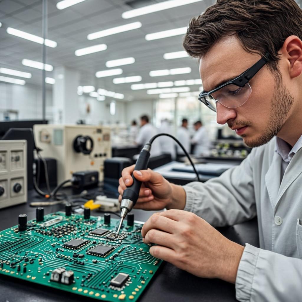
The multilayer PCB manufacturing process involves advanced stackup design, precise via formation, and rigorous quality control.
Key advancements in multilayer PCB manufacturing include miniaturization, HDI, flexible substrates, and embedded components. These improvements enhance stackup design and overall PCB performance.
A 4-layer pcb looks more complicated than single- or double-layer boards. It has at least three copper layers, with insulation between each one. In a 4-layer pcb, there are two signal layers and two inner layers. The inner layers are usually for power and ground. This design lets you fit more circuits in a small area. You can use different vias, like through-hole, blind, and buried vias. These vias help connect the layers and move signals between them. The inner layers often work as power or ground planes. This helps stop electromagnetic interference and makes signals clearer. You can see the differences in the table below:
You can find 4-layer pcb designs in many modern products.
Tip: Pick a 4-layer pcb if you need lots of parts, strong signals, and good performance in tough places.
When you pick materials for a 4-layer pcb, you must think about how it will work. The right substrate makes your multilayer pcb strong, bendable, and dependable. Here are the main substrates used in multilayer pcb manufacturing:
Tip: Picking the right material for multilayer pcbs helps you get the best mix of price, performance, and dependability.
Copper layers move signals and power in your 4-layer pcb. You must choose the right thickness for each layer in your multilayer pcb. Thin copper is good for inside layers. Thick copper is better for outside layers that carry more current. The table below shows common copper thicknesses used in multilayer pcb manufacturing:
New materials and methods are changing how you make a 4-layer pcb. Many multilayer pcb makers now use high-frequency dielectrics like Rogers for signal layers. They mix these with cheaper FR-4 for power and ground layers. This mix helps signals stay strong and saves money. Some companies use new via methods, like laser drilling, to make better connections. New resin systems and special low-loss materials can make high-frequency multilayer pcb boards up to 30% cheaper. Surface finishes like ENIG also make boards last longer, even if they cost more than old finishes.
You begin making a multilayer pcb by planning carefully. Good design helps you avoid mistakes later. Here are the main steps you should follow:
Keep all your design files and instructions neat and easy to find. This helps you make better boards and saves time.
Inner layer etching shapes copper on the inside layers. You use photoresist to protect copper you want to keep. Then, you spray chemicals to remove extra copper. Ferric chloride and cupric chloride are common chemicals. Ammonium persulfate is used for very careful jobs, but it works slower.
You must watch the speed, strength, and time of etching. This step is important for the rest of the process.
Stackup design is the base of every multilayer pcb. You put copper and insulation in a set order. A good stackup keeps signals clear and the board flat. Put signal layers next to power or ground planes. This helps signals and stops noise.
Use tools to check your stackup before building. A good stackup keeps signals strong and heat under control.
Lamination sticks all the layers of your pcb together. You stack prepreg and copper foil in the right order. Then, you press them with heat and pressure. The prepreg melts and glues the layers, pushing out air.
Drilling makes holes for vias that link layers. You use both machines and lasers. Lasers make tiny microvias for tight designs.
Place vias in smart spots to keep signals and power strong.
Plating covers holes and copper with a thin metal layer. This step makes sure layers connect with electricity. You must watch thickness, stickiness, and evenness.
Even plating keeps signals strong and the board working well. Check thickness and stickiness to make sure it is right.
Outer layer etching makes the final copper shapes. This step is harder than inner layer etching. You add photoresist, plate with tin, then remove extra copper. The tin keeps the copper you want.
Outer layer etching needs care to stop problems, especially for fast boards.
The solder mask protects your pcb from shorts and rust. It covers everything except the pads for parts. The most used solder mask is LPI. LPI gives sharp lines for small parts.
Watch the thickness and space of your solder mask. This stops solder bridges and helps place parts right.
Surface finish covers copper pads to stop rust and help soldering. You can pick from many finishes:
Pick the finish that fits your board, where it will be used, and your budget.
Silkscreen printing puts labels and numbers on your pcb. This helps you find parts when building or fixing. Follow these tips for good silkscreen: