HDI PCBs revolutionize circuit board design by packing more connections in less space. These advanced printed circuit boards enable smaller, more powerful electronics through their compact architecture.
Our facility is equipped to handle standard and complex multilayer PCB designs. The table below details our manufacturing capabilities.
For telecommunications and 5G applications involving high-speed signals, standard FR4 may cause signal loss. We utilize low-loss materials from brands like Rogers, Isola, and Panasonic to maintain superior signal integrity.
A well-planned stackup is the backbone of any multilayer circuit board. We assist engineers in calculating the correct dielectric thickness to achieve target impedance.
Once the layers are laminated, they cannot be repaired. Therefore, PCBinq employs strict controls:
AOI (Automated Optical Inspection): Every inner layer is scanned for open/short circuits before lamination.
X-Ray Inspection: Used to verify layer alignment and registration accuracy in high-layer-count boards.
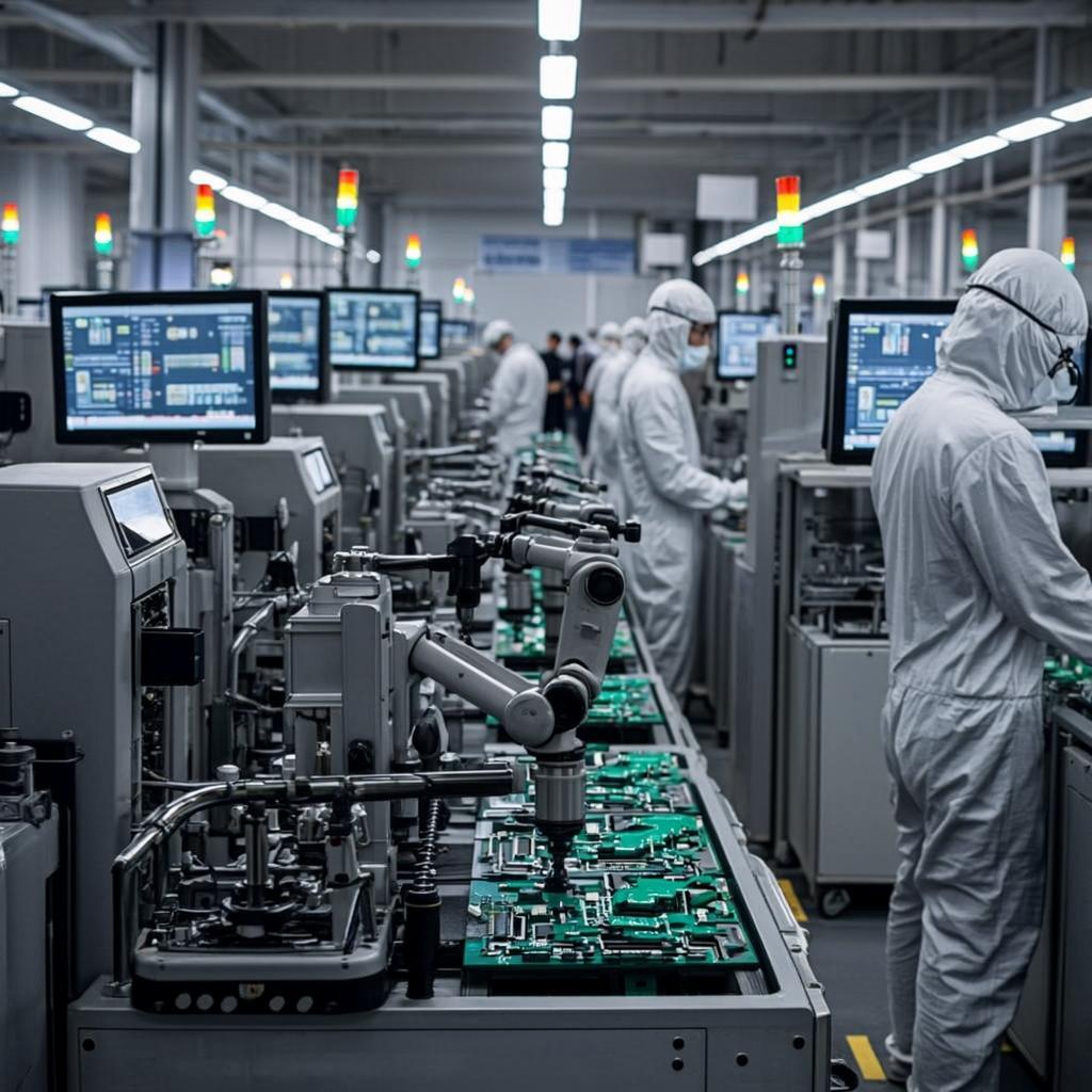
Manufacturing a multilayer circuit board is significantly more complex than producing double-sided boards. The process involves several critical steps that determine the final quality.
Inner Layer Imaging & Etching: We use advanced LDI (Laser Direct Imaging) to transfer circuit patterns onto the inner copper layers with high precision.
Black Oxide Treatment: Before lamination, inner layers undergo oxide treatment to increase surface roughness, ensuring a strong bond between the copper and the prepreg.
Lamination (The Critical Step): The layers are stacked with prepreg and pressed under high heat and pressure. We strictly control the temperature profile to prevent delamination and voids.
X-Ray Drilling: After lamination, we use X-Ray drilling machines to locate targets in the inner layers, ensuring that holes are drilled precisely through the center of the pads, accounting for any material shrinkage.
Whether you need a complex Any-Layer HDI design or a standard 6-layer circuit board, PCBinq is your trusted partner. Our engineers are ready to review your files.
The industry standard thickness is 1.6mm (0.062 inches), but we can fabricate boards ranging from 0.4mm to over 3.0mm depending on the layer count and application.
Cost increases with layer count due to additional materials (copper, prepreg), longer lamination cycles, and more complex manufacturing steps like visual inspection of inner layers.
For high-speed signals (like USB, DDR, or Ethernet), impedance control ensures the signal matches the source and load, preventing data errors and signal reflection.