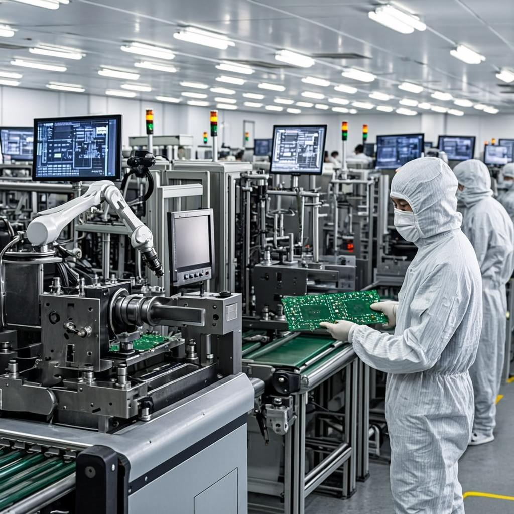
Blind Buried Circuits, a leading service provider of High-Density Interconnect Printed Circuit Boards (HDI PCBs), offers state-of-the-art technology solutions in electronic manufacturing. Our HDI PCBs manufacturing process supports designs with a higher density of components and interconnections in a compact form factor, which helps the designers achieve unparalleled performance, enhanced functionality, and reduced size of electronic devices.
Blind Buried Circuits offers advanced design and manufacturing solutions to achieve high- density interconnections. The design incorporates multiple layers of conductive material and vias, increasing routing density using micro, buried, and blind vias. This complex technology enables the interconnection of complex circuitry in smaller areas. The following are the benefits of HDI PCB technology:
In HDI PCB manufacturing, the stack of layers plays a critical role in ensuring optimal performance. A well-designed HDI board incorporates internal layers and stacked microvias that allow for high-density routing and efficient signal transmission. At Blind Buried Circuits, our engineers carefully plan the HDI board stack up, ensuring that each layer is precisely configured to meet the specific needs of your device, whether it’s for mobile technology or high-speed data transmission.
There is no comparison of HDI PCB vs Traditional PCB, as HDI PCBs are the better version of Traditional PCBs. Due to the limitation of routing density and interconnection capabilities of traditional PCBs, they are suitable for simple electronic designs with fewer component placements and interconnections. However, HDI PCBs enable greater design flexibility and complex circuitry.
At Blind Buried Circuits, we utilize cutting-edge techniques such as sequential laminations in our HDI manufacturing process. This method allows us to achieve higher circuit densities and improved performance, which is critical for industries requiring compact and powerful electronic designs. By incorporating microholes and other advanced fabrication techniques, we can create high-performance HDI PCBs that meet the demands of modern electronic devices.
Blind Buried Circuit manufacture all type of HDI PCBs. The following are the advantages of HDI PCBs:
Increased component density: For compact electronic devices, the circuits require a large number of components in a limited area. HDI PCBs can accommodate complex designs in limited areas.
Better signal integrity.