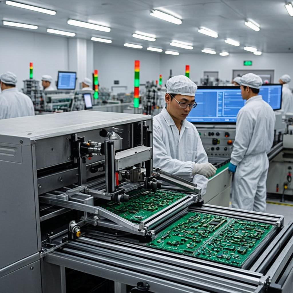
The multilayer printed circuit board (PCB) lamination process is a cornerstone of modern electronics manufacturing, enabling the creation of compact, high-performance devices like smartphones, medical equipment, and aerospace systems. Optimizing this process is critical to achieving reliable, high-quality PCBs that meet stringent performance requirements. In this blog, we explore the multilayer PCB lamination process, key optimization strategies, and practical tips to ensure superior outcomes for engineers and manufacturers.
Multilayer PCBs consist of three or more conductive copper layers separated by insulating materials, such as prepreg and core laminates. The lamination process bonds these layers into a single, cohesive board using heat, pressure, and precise alignment. This process is complex, as it must ensure electrical connectivity, structural integrity, and minimal defects like warpage or delamination.
The typical lamination process involves several steps:
Optimizing the lamination process directly impacts PCB performance, reliability, and cost. For example, poor lamination can lead to issues like:
By refining the process, manufacturers can achieve tighter tolerances, reduce defects, and improve yield rates, ultimately lowering production costs and ensuring boards meet industry standards like IPC-6012.
Choosing the right materials is foundational to successful lamination. The primary materials—prepreg, core, and copper foil—must be compatible in terms of thermal, electrical, and mechanical properties.
Compatibility is critical to avoid issues like coefficient of thermal expansion (CTE) mismatches, which can cause warpage. For instance, a CTE mismatch of >10 ppm/°C between layers can lead to significant stress during thermal cycling.
A symmetrical stack-up design minimizes warpage and ensures uniform pressure distribution during lamination. Key considerations include:
For a 4-layer PCB, a typical stack-up might include two signal layers on the outer surfaces, a ground plane, and a power plane, with prepreg layers of 0.15 mm thickness to ensure tight coupling and reduce EMI.
Precise control of lamination parameters—temperature, pressure, and time—is essential for consistent results. Recommended settings include:
Advanced presses, like the LPKF MultiPress S, use preset profiles to maintain these parameters, reducing defects in high-frequency multilayers. Monitoring the glass transition temperature (Tg, typically 130-180°C for FR-4) ensures the substrate remains stable during lamination.
Misalignment between layers can cause open circuits or shorts, especially in high-density designs. To optimize alignment:
For example, Rocket PCB recommends designing overlapping rivet holes for boards with 6+ layers to enhance alignment accuracy.
Common lamination defects include voids, delamination, and resin starvation. To prevent these:
Cross-sectional analysis can reveal defects like white edges (caused by low resin content) or bubbles, allowing process adjustments before full-scale production.
For high-frequency or high-reliability applications, additional optimization techniques are necessary:
These techniques enable boards to support signal speeds up to 10 Gbps while maintaining signal integrity and thermal stability.
At ALLPCB, we leverage advanced manufacturing capabilities to deliver high-quality multilayer PCBs tailored to your needs. Our state-of-the-art lamination equipment ensures precise control of temperature, pressure, and alignment, minimizing defects and achieving industry-leading tolerances. With support for 4 to 64-layer PCBs and a range of materials (FR-4, Rogers, ceramics), we provide customized solutions for applications from consumer electronics to aerospace. Our rigorous quality control, including AOI and thermal stress testing, guarantees reliable, high-performance boards that meet your exact specifications.
Optimizing the multilayer PCB lamination process is essential for producing reliable, high-performance boards that meet the demands of modern electronics. By focusing on material selection, stack-up design, process control, alignment, and defect prevention, manufacturers can achieve superior results. Advanced techniques like sequential lamination and low-Dk materials further enhance performance for specialized applications. At ALLPCB, we're committed to helping engineers navigate these complexities with cutting-edge solutions and expert support.