Email: pcb@frankenthalerfoundation.org Telephone: 0086-15919758327
We are creative, ambitious, and ready for challenges! Hire Us
HDI PCB is a multi-layer circuit board with high wiring density, thin lines, spaces and micro-holes. They are designed to increase the functionality and performance of electronic products while reducing their size. High-Density Interconnect (HDI) PCBs represent technological advancements in printed circuit board design and manufacturing. These boards are known for their enhanced electrical performance and compact size.
If necessary, you can click to view more of our cases.
begins with heat and pressure to layer and bond thin core materials to create a multi-layer stack.
Laser drilling and mechanical drilling can create micro vias and vias.
After drilling, copper is deposited on the hole’s walls to create a conductive path.
The photolithography process uses a layer of photoresist and ultraviolet light to define circuit patterns on each layer.
Chemically removing exposed copper, leaving the desired copper traces.
In the case of buried vias, any excess copper is filled and then planarized to create a flat surface.
Solder mask insulates and protects copper traces, while screen printing adds component labels.
The PCB’s surface undergoes surface treatment, such as ENIG (Electroless Nickel Immersion Gold) or HASL (Hot Air Solder Leveling).
With more than a decade of experience in the PCB industry, we have established a reliable supply chain that ensures quality components at competitive prices. For complex projects requiring unique materials or advanced technical specifications, our strong manufacturing capabilities enable us to provide cost-effective solutions while maintaining high quality.
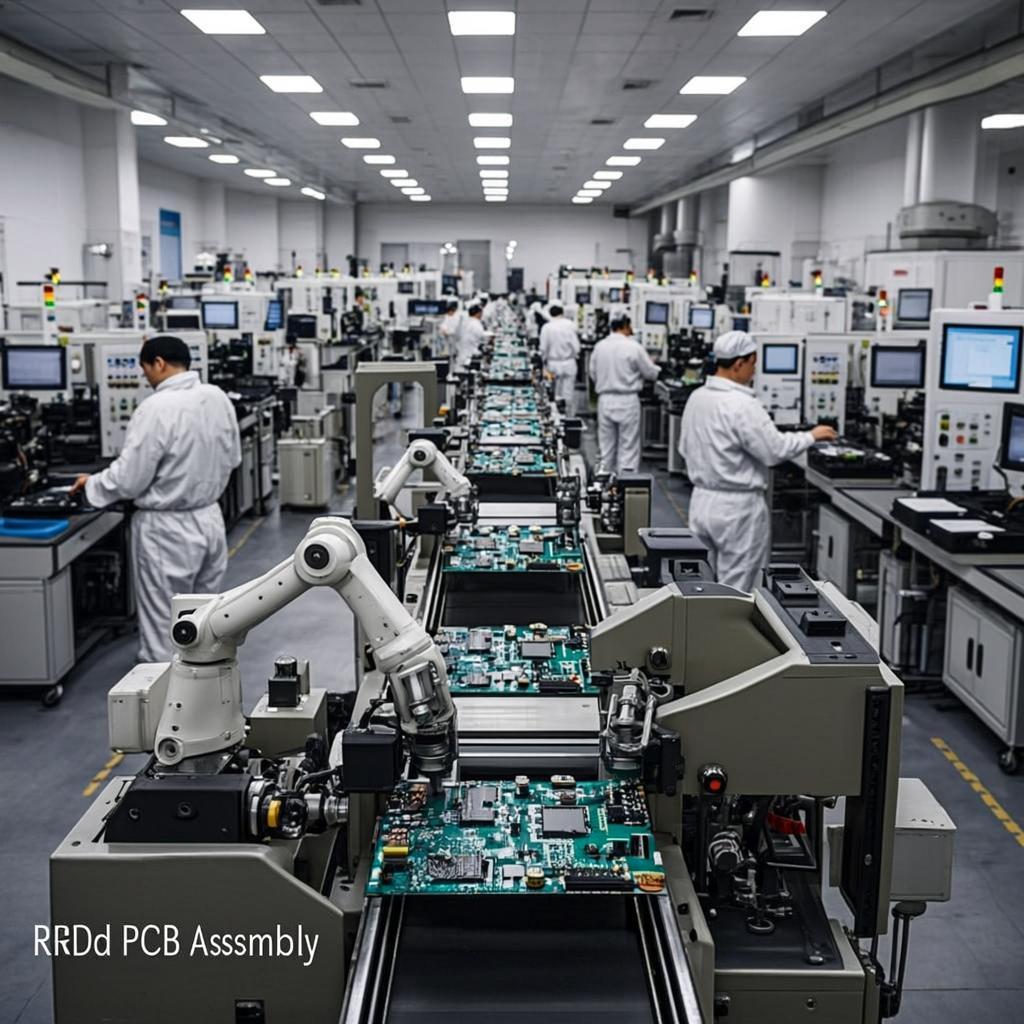
We ensure fast production and delivery. Our partnership with multiple global logistics providers guarantees timely and reliable transportation, supported by our digital factory management and 90% automation for greater efficiency.
Our rigorous quality inspection begins with incoming material checks. We use AOI to detect defects and X-rays to identify internal issues. Electrical performance testing is performed with advanced automatic test machines and flying probe testers. Before shipment, our dedicated QC team conducts a thorough manual visual inspection to ensure all products meet strict quality standards.
We also hold several international quality certifications:
At the same time, we are always committed to environmental protection. We have an environmental management system certification to ensure that our manufacturing process is environmentally friendly and sustainable.