01/ Cost Reduction This is the most important benefit of your long term relationship with us. After learning your specific needs, we will quickly work out a tailored integrated solution to meet your expenses and cost reduction targets.
02/ Certified Quality Standards Our quality assurance policy is not based on company integrity alone. It is also affirmed by various certifications recognized across North America. We are known for delivering only the best, most durable assemblies.
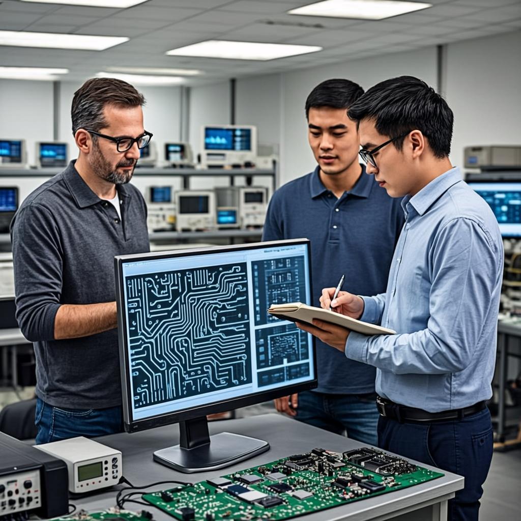
03/ Create Value for the Customer We work with our customers on an individual basis, making sure what we deliver matches your needs precisely. Moreover, we have a staff of Program Managers on board that help clients work out those needs, helping develop a raw idea into a comprehensive PCB Fabrication or PCB Assembly.
04/ Flexibility We react quickly to your changing needs. Our working time and style is flexible to meet your variable needs. To us, your requirements are our guidelines and rules to follow.
Thick copper PCBs are characterised by structures with copper thicknesses from 105 to 400 μm. These PCBs are used for large (high) current outputs and for optimisation of the thermal management. The thick copper allows large PCB-cross-sections for high current loads and encourages heat dissipation. The most common designs are multilayer or double-sided.
Quick Turn 2oz Copper PCB The ounce (oz) is a unit of weight and a unit of capacity. The conversion formula of ounces and
3 Oz Heavy Copper PCB Multilayer PCB with thick copper: our company has many production processes for the inner and outer
4oz Heavy Copper PCB 4oz=4OZ=140um=0.14mm copper foil thickness; high cost, PCB line width and line spacing are
10 oz copper PCB At the same time, as printed circuit boards are becoming more and more widely used in the
Ultra-high mechanical strength:After thick copper is applied to the circuit and vias of the board, the printed circuit board has ultra-high mechanical strength. Makes the weather resistance of the circuit board and the electrical system more stable. It can be used in hot melt welding methods such as oxygen blowing at a high melting point and not brittle at low temperatures. Even in extremely corrosive atmospheric environments, copper weight PCB forms a strong, non-toxic passivation protective layer.
Excellent weather resistance:Due to the heavy copper PCB board supports the choice of various dielectric materials. It can ensure the stability of the circuit transmission signal under some high temperature or extreme special environment. Special dielectric materials improve the overall weather resistance of the board.
Thermal Management:With the advancement of modern technology, PCBs are becoming more and more complex. The high density of current increases the difficulty of thermal management. Excessive temperature can affect the normal operation of electronic equipment, and even cause damage. The thick copper PCB board can provide stronger heat dissipation capability. Matching heatsinks and adding copper plating to through holes can drastically reduce board heat.
Excellent current conduction:In the operation of electronic equipment, the heavy copper printed circuit board is an excellent current conductor. It can be connected to transmit electricity between various boards.
Diversity:Its conductive materials, substrate materials, production process, application fields are different from the standard PCBs. The plating of thick copper circuits allows heavy copper PCB manufacturers to increase the copper weight in via sidewalls and plated holes, which can reduce the layer numbers and footprints.
Extendability:Thick copper PCB has the best elongation performance and is not limited by the processing temperature.
High performance: Thick-copper plating integrates high-current and control circuits, making high-density with simple board structures can be achieved.
The manufacturing process of thick copper PCB follows almost similar steps of standard PCBs and the only difference apart from the standard one is the thickness of copper used. Following is the step-by-step manufacturing process which is implemented:
Design:The design or layout of the PCB to be manufactured is drawn out of specific designing software according to the specific requirements of circuits. While designing, make sure that the design meets the electrical and thermal requirements as well as the thickness of the copper used.
Choosing the Substrate material: Substrate materials are usually selected based on their ability to handle a thick copper layer. For that reason, the material used is usually a high-temperature FR-4. By using electrodeposition or lamination techniques, a thick copper foil is applied to the substrate. The thickness of the copper layer here is usually greater than 2 oz (ounces) or 70 micrometres.
Lamination:It is the next step which involves copper layers pressing together using heat and pressure to build a strong board. This process assures good adhesion between the layers.
Drilling:Holes are drilled into the board according to the PCB design in particular locations. These holes allow the interconnection between layers and will hold the electronic components together.
Through-Hole Plating:For creating a strong and dependable circuit, this step is really important. This is the process of plating conductive material along the drilled holes in order to create electrical connections.
Circuit imaging:A photosensitive material called resist is enforced over the copper layer and it is then exposed to UV light through a mask which is of the PCB layout. This will form the circuit pattern of the PCB.
Etching:The exposed copper protected by the resist stays behind and the copper which is not protected by the resist is etched away using a particular chemical solution. Through this process, we can leave the intended copper traces on the PCB.
Surface Finish:This process will prevent PCBs from oxidation and improve the solderability of the exposed copper traces. There are some commonly used surface finishes such as Hot Air Solder Leveling (HASL), Organic Solderabili