Designing RF PCBs is important for modern technology like phones and car radar. These boards work with signals over 1GHz to keep them clear and strong. Unlike regular PCBs, RF boards need special materials to avoid signal loss at high speeds. You must solve problems like matching signal paths, stopping signal bounce, and blocking unwanted noise. Careful planning and following good design rules are key for success. Learning RF PCB design helps create advanced and exciting technologies.
RF PCB design is about making circuit boards for high-frequency signals, usually above 1 GHz. These boards are used in things like wireless devices, radar, and IoT gadgets. Unlike regular boards, RF designs need exact control of signal paths and impedance to keep signals clear.
Important parts of RF PCB design include:
You also need to plan the return signal path carefully. This avoids problems with mismatched impedance. As boards get more crowded, crosstalk becomes a bigger issue. To fix this, you must space traces properly and plan layouts well.
Tip: Focus on matching impedance and cutting noise for better RF results.
RF PCBs are different from regular PCBs in key ways. The dielectric constant (Dk) of the material is very important in RF design. It affects how signals behave. But Dk values can change between manufacturers because of different testing methods. This makes picking materials harder.
RF designs also react more to material properties at higher frequencies. For example, laminate materials affect both the traces and the board’s electrical performance. This is even more critical in precise systems like military applications.
Note: Check Dk values from manufacturers and understand their testing methods before choosing materials.
High-frequency signals in RF PCBs act differently and need special care. Small parts like resistors and capacitors can behave unpredictably at high frequencies. For instance, resistors may not match their labeled values at around 10 GHz.
To handle this, use detailed data like impedance graphs or S-parameter charts. These tools show how parts work at certain frequencies. This helps you design more accurately and avoid surprises.
Tip: Use data to check part performance and prevent signal issues.
Picking the right materials is very important for RF PCB boards. Materials need steady electrical properties, especially at high frequencies. The dielectric constant (Dk) helps signals move through the board. A stable Dk makes signals act predictably, which is key for high-frequency use. The dissipation factor (Df) shows energy loss. Materials with low Df reduce signal weakening.
Heat is another thing to think about. High-frequency signals create heat that can change material properties. This hurts performance. Materials like PTFE laminates handle heat and keep electrical properties steady. These are often used in RF devices like base stations.
Tip: Check material specs like Dk, Df, and heat stability from manufacturers.
Key things to check include:
Impedance control is very important in RF design. It keeps signals moving without bouncing or losing strength. If impedance doesn’t match, signals bounce back and cause problems. RF boards need steady impedance, usually 50 ohms, for best results.
Impedance tests show if the board matches expected values. Good impedance control stops signal bouncing and improves electromagnetic compatibility. For example, it reduces electromagnetic interference (EMI), which helps RF circuits work better.
To control impedance, design trace widths, spacing, and layers carefully. Simulation tools can predict impedance and help improve the design before making the board.
Note: Impedance control is a must for RF boards. It affects signal quality and circuit performance.
Signal integrity and EMI are connected in RF design. High-frequency signals can easily get interference, which messes up signals. When traces are close, crosstalk and noise happen more often. To fix this, keep traces apart and use shields like ground pours and via stitching.
For example, ground pours and via stitching can cut coupling by 20 dB. This improves signal integrity by 100 times. Shielding cans, which cover most of the PCB, also block interference. But small designs may not have space for these.
Heat noise and RF path loss also hurt signal integrity. Fix these by improving layouts and using parts made for high frequencies. Simulation tools help find problems and check your design.
Tip: Use shielding and good layouts to protect signals and lower EMI.
The layer stack-up in an RF PCB is very important. It shows how copper and dielectric layers are arranged. This affects signal quality, impedance control, and electromagnetic interference (EMI).
The stack-up decides how signals move through the board. A bad stack-up can cause signal loss, crosstalk, and EMI. Planning the layers well helps avoid these problems. It also keeps RF circuits working reliably.
Tip: Think about frequency and material properties when planning the stack-up.
When designing the stack-up, focus on these parts:
Use these tips to make a strong stack-up for your RF PCB:
Here’s an example of a 4-layer RF PCB stack-up:
This setup keeps signals clear and lowers EMI.
Note: For complex designs, add more layers to separate signals and power planes.
Use software like Altium Designer or KiCad to design your stack-up. These tools let you test your design and fix problems before making the board.
By planning the layer stack-up carefully, you can make RF PCBs work better for high-frequency uses. This step is key to avoiding signal problems and ensuring good performance.
Before starting, set clear goals for your RF PCB. These goals act like a guide to help your design meet performance needs. Focus on important factors to make good decisions.
To meet these goals:
Tip: Make a checklist of your goals before you start. This helps you stay focused and avoid mistakes.
Picking the right materials and parts is very important. The materials you choose affect how the board works, especially at high speeds. Look for materials with steady dielectric constants (Dk) and low dissipation factors (Df). These help signals stay clear and reduce energy loss.
For example, PTFE laminates are great for RF boards because they handle heat well and lose less signal. When choosing parts, check how they work at high frequencies. A resistor might not work as expected at 10 GHz. Use data sheets with graphs to confirm how parts perform.
Note: Talk to manufacturers to make sure materials and parts fit your needs.
Things to think about when picking materials and parts:
The layout is where your design becomes real. Following good layout rules is key to making your RF PCB work well. Keep high-frequency traces short and direct. This lowers signal loss and interference.
Use ground planes to give signals a steady base and control impedance. Placing signal layers near ground planes improves signal quality and cuts interference. Add via stitching and ground pours to protect sensitive areas even more.
Tip: Advanced layout methods can improve performance by 10 to 30 times. Try new techniques to make your design better.
Other layout tips include:
By planning your layout well, you can avoid problems like signal issues and EMI. This ensures your RF PCB works well in high-frequency situations.
Testing your RF PCB design with simulations is very important. It helps find and fix problems before making the board. This saves both time and money. Simulations show how high-frequency signals behave and check if the design works well.
High-frequency signals are sensitive to layout and materials. Without testing, you might face signal loss or interference. Simulation tools let you spot these problems early. You can adjust your design to avoid issues like mismatched impedance.
Try these methods to test your RF PCB design:
Tip: Use more than one simulation method for better results.
Pick tools with these features for better testing:
Simulation tools also help find noise and power issues. For example, they can check stackups and power stability. This helps improve your design and fix weak spots.
Note: Always test your design under real-world conditions for accuracy.
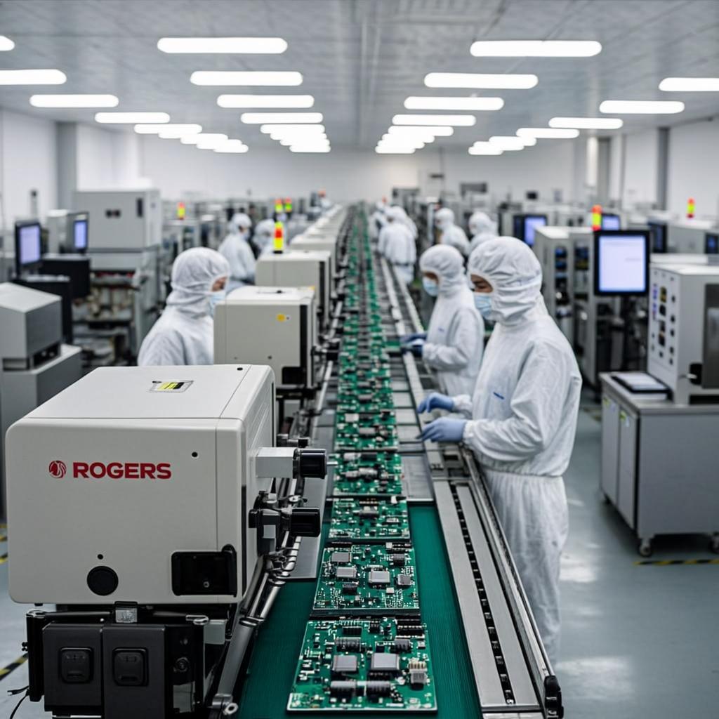
Once your design is ready, it’s time to make and test the board. This step ensures the RF PCB works well and meets quality standards.
Work with your manufacturer to match your design needs. Share clear details like material types and impedance goals. This reduces mistakes during production.
To check quality, make a few sample boards first. Produce 5–25 boards to test how consistent they are. This helps find any problems in the manufacturing process.
Testing makes sure your RF PCB works as planned. Follow these steps to test it: