Polytetrafluoroethylene (PTFE) PCBs are integral to advanced electronic applications. Among various PCB materials, Teflon, the brand name for Polytetrafluoroethylene (PTFE). Teflon PCBs, known for their high frequency and heat resistance properties. All of this is achievable due to its exceptional dielectric properties. RF PCB designs often make use of low-loss PTFE-based materials thanks to their very low dielectric losses and huge range of possible Dk values.
From their initial application in military technology during the mid-20th century to their current use in advanced communication systems, Teflon PCBs have revolutionized the way we perceive and develop electronics. This blog will explain Teflon PCB in detail, its materials, importance, applications, specifications and all the advantages that it adds to the industry. To know more about advanced PCBs see our latest article on multilayer PCB design.
PTFE is a synthetic fluoropolymer widely recognized under the brand name Teflon. Its non-reactive nature, low dielectric constant, and superior thermal resistance make it an ideal material for specialized PCBs. This type of PCB is specifically designed to transmit signals at frequencies of 5GHz and above, making it an optimal choice for microwave and RF applications. It has low moisture absorption, and is therefore perfect for settings that need reliability and strong performance. PTFE materials also require additional care during PCB Fabrication due to a few specific aspects of the material itself, relative to standard FR-4. Have a look at the dielectric, conductivity and loss tangent factors of some of the following PTFE base materials.
Compared to standard FR4 PCBs, PTFE PCBs are better suited for applications requiring low loss, high-frequency transmission, and environmental resilience. While more expensive, the performance benefits justify their use in high-end technology.
However, despite their advantages, Teflon PCBs may not be the best choice for every situation. Here are a few factors to consider when deciding whether to use a Teflon PCB or an alternative, here is the chart of available options for PTFE in JLCPCB fabrication lab.
Teflon PCBs are favored in scenarios that require superior frequency and temperature endurance. Here are some defining attributes of this type of printed circuit board:
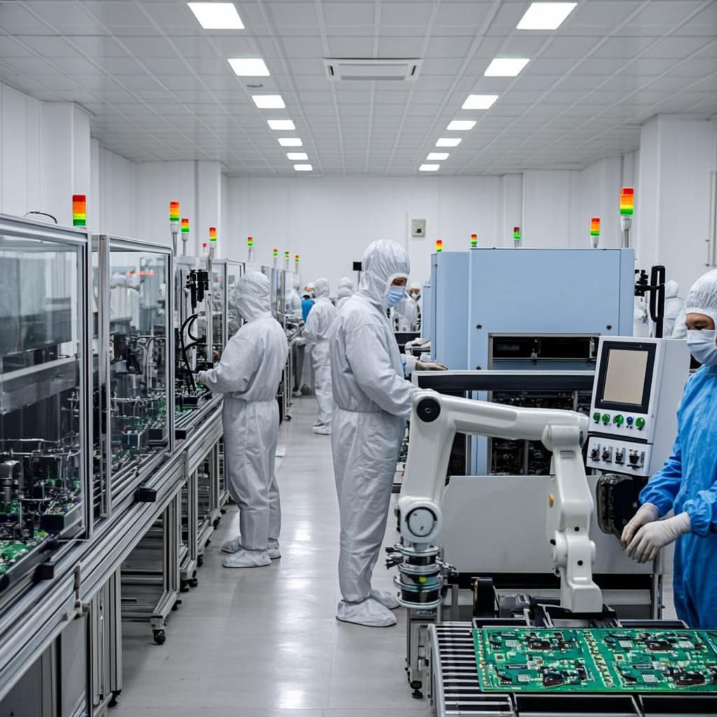
Crafting Teflon circuit boards demands a high level of precision and attentiveness. Manufacturers specializing in Teflon PCBs recognize the distinct differences between Teflon and standard FR4 PCB materials. The key manufacturing steps involved in the production of Teflon boards are as follows:
PTFE laminates are the foundation of Teflon printed circuit boards; these laminates are frequently reinforced with ceramic fillers or glass fibers. These materials offer the high-frequency applications the required mechanical stability and strength.
Carefully cleaning the PTFE laminates is necessary to get rid of any impurities that could interfere with the copper layers' adherence. The selection of tools used in surface preparation is crucial. Manufacturers avoid using bristles, scrubbers, and composite brushes, which could potentially damage the delicate laminate.
Vacuum pressing is the process of laminating copper foil onto a PTFE substrate under vacuum utilising pressure and heat. Reliable operation depends on a strong, homogeneous binding between the copper and PTFE, which is ensured by specialised vacuum presses. Teflon PCBs require careful copper plating. PTFE materials have a high Z-axis coefficient of thermal expansion, and need optimal pressure.
The copper-clad PTFE laminate is coated with a photoresist layer. The circuit layout is defined by a photomask that exposes this layer to UV light. The exposed photoresist is developed, and the desired circuitry is left intact by etching away the undesired copper with chemical solutions.
It's crucial to apply the solder mask within 12 hours of etching the material. Manufacturers process the etched surface via a standard PTFE cycle, ensuring any residual moisture is eliminated by baking the PTFE laminates before solder mask application.
High precision drilling of vias and component leads guarantees precise positioning and dependable connections. PCB fabricators often favor ceramic-filled laminates due to their ease of drilling. The copper plating of the drilled holes creates electrical connections between the PCB's several layers.
Electrical testing is performed to ensure general operation and to look for short circuits and open circuits, thorough electrical testing is carried out. Visual inspection gives an in-depth visual assessment guarantees the absence of flaws or contradictions. It's recommended to store them at room temperature, away from sunlight, to prevent surface oxidation and contamination.
For procedures like laminating, etching, and plating to produce the best results, skilled manufacturers know exactly what has to be done. The success of producing Teflon PCBs depends on the application of certain machinery and procedures together with the knowledge and experience of qualified producers. Production of dependable, high-quality PCBs that can function in the most demanding settings is ensured by this combination.
In the world of PCBs for RF electronics, PTFE is better known as the material of choice for many RF systems. For high-frequency applications, Teflon PCBs with their low dielectric constant and dissipation factor guarantee less signal delay and electrical loss. Their remarkable dependability is derived from their minimal moisture absorption, chemical resistance, and great thermal stability. Teflon PCBs are essential in modern communications, aerospace, and industrial applications For manufacturers, high-frequency performance and environmental endurance should be the top priorities while using them.