Fluoropolymer PCBs using Teflon/PTFE with ultra-low loss (Df <0.001 @ 10 GHz — less than zero point zero zero one), stable Dk, ±3–5% (plus/minus three to five percent) impedance control, VNA/TDR validation, and hybrid stackups with FR-4 or ceramic.
Low dielectric loss, stable Dk and predictable phase
Teflon/PTFE substrates provide ultra-low dielectric loss (Df 0.0009–0.0015 — zero point zero zero zero nine to zero point zero zero one five) and stable dielectric constant (Dk 2.1–2.3 — two point one to two point three), maintaining phase and insertion-loss control up to 40+ GHz (forty gigahertz and beyond). Compared with FR-4 PCB, fluoropolymer systems sustain consistent performance through RF, microwave and mmWave regimes where glass-epoxy laminates struggle.
For cost and manufacturability balance, most designs use hybrid stackups—placing PTFE only on RF signal layers and using FR-4 for inner planes—cutting material cost by 30–50% (thirty to fifty percent). These configurations integrate seamlessly with Rogers PCB and high-frequency PCB designs. See also our notes on microwave loss budgeting and stackup design.
Critical Risk: PTFE’s low surface energy and soft mechanical properties make bonding, hole-wall integrity, and dimensional stability challenging. Poor plasma activation or excessive drill heat can cause delamination or resin recession, degrading impedance uniformity.
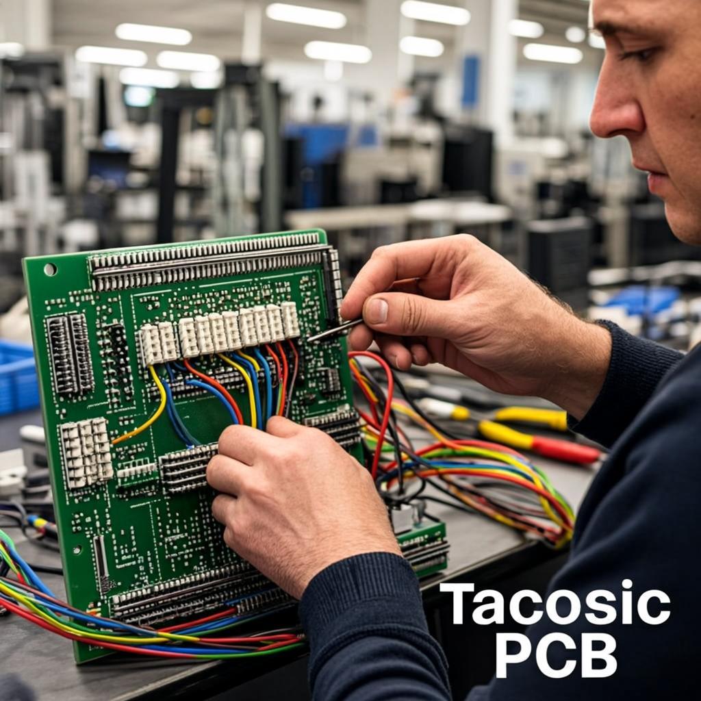
Our Solution: We use plasma activation and controlled oxidation to promote adhesion between PTFE and copper foils. Bonding layers employ high-temperature prepregs with CTE-matched glass fabrics. Laser or micro-drilling at reduced chip-load preserves via quality, and etch compensation maintains impedance within ±5% (plus/minus five percent). Each lot undergoes TDR verification and impedance correlation to confirm compliance with RF design targets.
For advanced mmWave and hybrid RF/digital assemblies, we combine PTFE surfaces with ceramic-filled or low-roughness copper laminates—learn more in our PTFE bonding guide and via drilling optimization overview.
Plasma activation, staged lamination, controlled drilling
PTFE/Teflon are chemically inert and require plasma activation for reliable hole-wall adhesion. We use staged temperature/pressure lamination and controlled drilling to avoid smearing. UV-laser microvias (75–100 μm — seventy-five to one hundred micrometers) and backdrill remove resonant stubs for 25+ Gbps channels.
Verification includes TDR (±3–5% impedance — plus/minus three to five percent), and sample-based VNA S-parameters up to 40 GHz (forty gigahertz). See high-frequency testing and impedance testing for methodology.
Process aligned with IPC-6018-style workflows for high-frequency PCBs
Ready to start your PCB project?
Whether you need simple prototypes or complex production runs, our advanced manufacturing capabilities ensure excellent quality and reliability. Get your quote within 30 minutes.
Use rolled/VLP copper to lower conductor loss by ~10–25% (ten to twenty-five percent). Keep return-via fences within ~1× (about one times) via diameter and consider backdrill so residual stubs are <10 mil (less than ten mils). Model copper roughness in solvers and validate with coupon impedance testing. For tight space, combine with HDI microvias to control launch geometry.
Our engineering team provides free DFM analysis and optimization recommendations
Sample-based VNA characterizes S11/S21 commonly up to 40 GHz (forty gigahertz), while TDR verifies impedance within ±3–5% (plus/minus three to five percent). PTFE’s moisture absorption is typically <0.01% (less than zero point zero one percent), stabilizing Dk/Df under humidity swings. For long links or backplanes, coordinate with High-Speed PCB to budget loss and reflections.
77 GHz automotive radar, 5G/6G radios and phased arrays, SATCOM (Ka/Ku-band), precision test fixtures and low-loss interconnects. For thermal paths or power RF, consider ceramic PCB or metal core PCB on select layers in a hybrid stack.
Experience: RF builds with coupon-to-solver correlation and staged lamination windows for fluoropolymers.
Expertise: plasma activation, rolled/VLP copper selection, controlled-depth drilling and backdrill.
Authoritativeness: workflows aligned with IPC-6018; documentation/audits supported for AS9100/MIL-PRF programs.
Trustworthiness: MES traceability links lot IDs, coupons and test data; reports available upon request. See HF testing methods and advanced RF design.
Select PTFE/Teflon when operating at RF/microwave/mmWave where very low loss and phase stability are critical. Use hybrid stacks to keep PTFE only on RF layers and FR-4 elsewhere for cost efficiency.
Yes. We provide sample-based VNA S11/S21 and coupon-based TDR. Production lots include electrical data as specified.
We backdrill to residual stubs under ten mils and can add controlled-depth drilling or HDI microvias to optimize launch transitions.
Rolled/VLP copper reduces roughness-induced loss; ENIG or Immersion Silver offer flat, low-roughness pads. ENEPIG is preferred for wire-bond or mixed RF/analog.
Yes. We routinely build hybrids to balance RF performance and cost, and we coordinate documentation for AS9100/MIL-PRF programs on request.
Experience Advanced PCB Manufacturing Excellence
From simple prototypes to complex production runs, our world-class factory delivers superior quality, fast turnaround and competitive pricing. Join thousands of satisfied customers who trust us with their PCB manufacturing needs.