A multilayer PCB refers to a circuit board that has more than two conductive layers, allowing enhanced functionality within limited space. At present, multilayer PCBs are used by almost every industry. Various consumer electronic devices, automotive solutions, medical equipment, defence and space technology, and industrial automation are using advanced and multi-functional devices. The materialising of these devices is only possible due to the introduction of multi layer circuit board technology.
Due to the complexity of multi-layer PCBs, we need to understand the layers they consist of.
As the name specifies, a multilayer PCB consists of layers with different properties in greater numbers. Each layer is defined as part of the entire circuit layout. Core layer, prepreg layer, and conducting layer are major categories of the multi-layer. Based on the circuit layout, conducting layers are further classified as power layer, ground layer, or signal layer.
To make various interconnections into a multilayer printed circuit board, the arrangement of vias and interconnections is provided with a perfect combination. Vias can be of blind or buried type, depending on the design considerations. To maintain the circuit continuity, several interconnection arrangements are made between the internal layers. Power and ground layers serve as the main source of power & ground for all the layers at the required points.
As every layer incorporates a selected function in a multilayer PCB board, the layer stackup becomes a critical point during the design and manufacturing process. For example, a typical 7-layer PCB setup can be in the form of top, power, signal, ground, signal, and power & bottom layer. Any mismatch in the order of the required PCB layer stackup will result in the failure of the entire multilayer circuit board.
Each circuit works on some input conditions and generates a respective output for the end application. Since a multilayer PCB board has its circuit divided into various sections, setting up the terminals for input & output becomes important. In some applications, internal response or feedback is also required. Dedicated arrangements are provided in the PCB stackup for this purpose. The interconnection of the internal layers is also done with suitable components to avoid any signal interference and loss in multi-layer PCB boards.
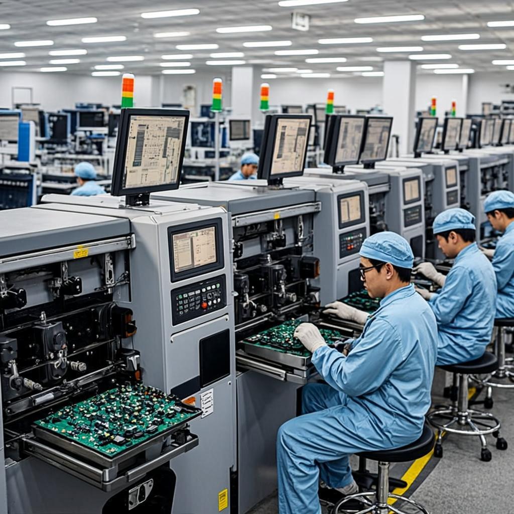
Every step in the manufacturing process of multilayer PCBs is indispensable. The absence of any step or an error in operation will result in the produced PCBs not meeting the desired requirements. Therefore, it is crucial to have a thorough understanding of the manufacturing process of multilayer circuit boards.
Be it single-layer or multi-layer PCBs, any PCB manufacturing project starts with its design process, where the required circuit is transformed into a production format. All the layers, tracks, vias, holes, component packages, layer width, material selection, and many parameters are decided and finalised into a reliable design to produce. Complete design documentation is also done for the reference and usage of the manufacturing and assembly units. A well-designed multilayer PCB stackup also reduces EMI effects and improves overall electrical performance.
While designing any kind of PCB, adherence to IPC standards and specifications is quite crucial. For example, IPC-4101 specifies core material requirements. Using the defined materials for laminates and prepregs ensures proper bonding for the multilayer PCB board. Irrespective of your PCB requirement, IPC standards are non-negotiable. Hence, make sure your manufacturer sticks to all the applicable ones while designing your PCB. Additionally, run a DFMA (Design for Manufacturing and Assembly) test before moving on with the manufacturing process.
Since multiple layers are stacked over each other to form a compact product, the stacking is important during PCB manufacturing. The thermal management of the PCB is one of the key considerations during multilayer PCB operation. For this, high thermal grade material is used in the inner layer preparations. Mechanical stress also affects the PCB integrity, which is also taken care of during the assembly stages.
In single or double layers, drills are done directly on the PCB surface. But for multilayer Printed Circuit Boards, drilling is required to be carried out with utmost care due to the limited width and the presence of the next layer underneath. After drilling, suitable electroplating is applied over the drilled holes and outer surface to maintain the right electrical continuity.
Outer layers undergo the resistive coating to protect the multi layer circuit boards from external factors. A layout for the resistive coating is prepared and developed accordingly on the PCB surface. The excess amount of coating is further etched and stripped from the PCB surface with a proper cleaning process.
To save solder from oxidation and other defects, solder mask is applied to the PCB. Silkscreen is also implemented on the PCB surface to provide adequate data about the components and PCB parameters. To end the process with a very last surface finish, various methods like HASL, ENIG & OSP are applied to the multilayer PCB assembly process.
The overall quality of the PCB is the most relevant point for any end application. The PCB is checked at each level of the manufacturing and assembly for any quality defects by various methods. Here, the inspection for internal layers is more typical and needs to be carried out with quite precision. Final electrical testing is required to verify the electrical parameters of the multi layer PCB.
Manufacturing a multilayer PCB is a complex process that requires utmost precision and expertise. One small negligence at any step may lead to non-functional or faulty circuit boards or PCBs with a short life span. Therefore, to save your time and money, trust certified multilayer PCB manufacturers, like Viasion, only.
Since the introduction of multi-layered PCB boards, one way or the other, they have been used extensively by almost all industries. The wide range of functionality, ability to be customised, and enhanced performance of multilayer circuit boards make them a popular choice for electrical and electronic goods across all technologies. Below are some industries that make good use of this invention.
Besides, other industries, viz, automotive, telecommunications, computer electronics, aerospace, military and defence, science and research, etc., use multi-layer circuit boards one way or the other. So, no matter what your niche is, consult the experts at Viasion to find out if a multilayered PCB is the right choice for your project!
Before moving on, in case you are wondering, ‘what is the difference between a multilayer PCB and a double-layer PCB’, do not skip this section of the guide!
Firstly, let us understand what a double-layer PCB is. Often called a ‘double-layer’ PCB, this PCB is, in fact, composed of a single-layer substrate with circuits (copper layers) on both sides of the PCB board. Hence, they are commonly known as double-sided PCBs in the industry.
Such PCBs can accommodate more components than a single-sided PCB, but much fewer than a multi-layered PCB board. This reduces the cost of manufacturing; however, limits its applications as well. Below is a simplified comparison among different types of PCBs based on the number of layers/sides.
The major advantage of having a multilayer PCB is to integrate larger & complex circuits into compact dimensions. Various parts of the circuit can be divided into layers by maintaining the form factor of the PCB. Due to reduced dimensions, power & signals travel shorter distances, which provides good signal integrity. Multiple layers of power, ground, and signals provide design flexibility and design optimisation in the best ways. The overall weight also gets reduced in a multi layer circuit boards.
Regardless of having many advantages, the multilayer PCBs may have a few obstacles for PCB owners. The manufacturing price of the multilayer circuit board is high due to design complexity and material selection. High precision is required during manufacturing & assembly, which increases the overall production time significantly. Having an internal layer makes it complicated to repair the multilayer PCB in case of failures. Also, if the layers are not stacked well, the thermal stress can cause major harm to the PCB structure.
The abilities of multilayer circuit boards, such as compactness with higher performance, flexibility, durability, and lightweight production, make them suitable for various fields. This is making them an integral part of modern electronics. If your application requires similar features, a multilayer PCB might be the right choice for you.
Further, this technology is rapidly evolving with high-density structures, advanced materials, lower form factor, and improved performance. Therefore, make sure you partner only with a trusted multilayer PCB manufacturer , like Viasion, who adheres to IPC standards and prioritises quality control. To get a custom-designed quote for your application, consult our team today.