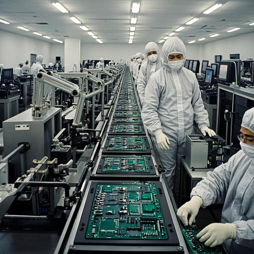
Compare to standard Rigid PCB, HDI PCB request much higher wiring density with finer trace and spacing, smaller vias and higher connection pad density. Blind and buried vias'design is one of their marked feature.HDI PCB are widely used for Cell Phone, tablet computer, digital camera, GPS, LCD module and other different area. The advantages of HDI PCB include:
Currently the advanced HDI technology we used include: "Copper Filled" for special stack microvia, "Laser Direct Imaging"(LDI) is specifically designed for fine line technology, to eliminate dimensional stability problem of artwork caused by environmental and material issues. "Direct Laser Drill"(DLD) is drilling of copper layer by direct CO2 laser irradiation, compare to additional laser drilling with conformal mask, the copper direct laser drilling is capable of providing higher accuracy, better hole quality and better efficiency for HDI projects
A-Tech Circuits Co., Ltd.
Tel: +86 (755) 2335-9039
Fax: +86 (755) 2306-4829
Email: pcb@frankenthalerfoundation.org
Welcome to contact us online
Copyright © 2012 - 2026 A-TECH Circuits Co., Ltd. All rights reserved. Web design by NewLoong
Address: 602, Building B3, Zhimei Huizhi Industrial Park, Fuyong Street, Bao'an District, ShenZhen City, China.
Tel: +86 (755) 2335-9039 Fax: +86 (755) 2306-4829 E-mail: pcb@frankenthalerfoundation.org