Printed Circuit Board (PCB) assembly is the backbone of modern electronics, powering everything from smartphones and medical devices to automotive systems and industrial equipment. At JHYPCB, we specialize in delivering high-quality PCB assembly services, including prototype PCB assembly, low-cost PCB assembly, quick-turn PCB assembly, turnkey PCB assembly, lead-free PCB assembly, and SMT stencil fabrication. Whether you’re a designer creating innovative prototypes, a procurement professional sourcing reliable manufacturing solutions, a beginner exploring PCB technology, or a business seeking scalable production, understanding the PCB assembly process is essential to achieving your project goals.
PCB assembly (PCBA) transforms a bare circuit board into a functional electronic system by mounting and soldering electronic components onto it. This intricate process involves advanced techniques like Surface Mount Technology (SMT), Through-Hole Technology (THT), and mixed technology, tailored to meet diverse application needs. From rapid prototyping for startups to high-volume production for established manufacturers, JHYPCB offers comprehensive solutions that ensure precision, efficiency, and cost-effectiveness.
In this guide, we’ll walk you through the complete PCB assembly process, from design and component placement to testing and delivery. You’ll discover how JHYPCB’s state-of-the-art facilities, certified by RoHS, UL, and ISO, deliver quick turn PCB assembly for urgent projects, turnkey PCB assembly for end-to-end convenience, and lead-free PCB assembly for eco-friendly compliance. Whether you need a custom SMT stencil for precise solder paste application or a low-cost solution for high-volume orders, JHYPCB is your trusted partner. Let’s dive into the world of PCB assembly and explore how we bring your electronic designs to life.
Printed Circuit Board Assembly (PCBA) is the process of transforming a bare PCB into a functional electronic system by mounting and soldering electronic components onto its surface. A bare PCB consists of a non-conductive substrate with conductive traces, designed to form electrical pathways. In contrast, PCBA involves the precise placement and connection of components—such as resistors, capacitors, integrated circuits (ICs), and transformers—to create a complete, operational circuit used in devices like smartphones, medical equipment, or industrial systems.
The PCBA process requires expertise in component placement and soldering techniques to ensure reliable electrical connections and optimal performance. Various methods, including Surface Mount Technology (SMT) and Through-Hole Technology (THT), are employed based on the design requirements. PCBA is critical for turning a conceptual circuit design into a practical product, making it a cornerstone of modern electronics manufacturing.
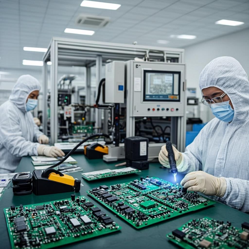
PCB assembly employs different techniques to mount electronic components onto a printed circuit board, each suited to specific design requirements and applications. The three primary types of PCB assembly are Surface Mount Technology, Through-Hole Technology, and Mixed Technology. Each method offers unique advantages and is chosen based on factors like circuit complexity, durability needs, and production scale.
Surface Mount Technology involves mounting components directly onto the surface of a PCB using solder paste. Unlike traditional methods, SMT eliminates the need for drilled holes, allowing for smaller, lighter, and more compact designs. Components, such as resistors, capacitors, and integrated circuits, are placed on contact pads and secured through reflow soldering, a process that melts solder paste to form reliable connections. SMT is highly automated, enabling high-speed production and precision, making it ideal for modern electronics like smartphones, medical devices, and consumer gadgets. Its advantages include reduced board size, higher component density, and lower production costs for large-scale manufacturing.
Through-Hole Technology, an older method, involves inserting component leads into pre-drilled holes on the PCB, which are then soldered on the opposite side to form connections. This technique is known for its robust mechanical bonds, offering high durability and resistance to heat and stress. THT is often used for components requiring strong physical connections, such as connectors or transformers, and is common in applications like industrial controls or simple devices like digital clocks. However, THT is less suited for multilayer PCBs due to the complexity of drilling and lower component density, making it less efficient for high-volume production compared to SMT.
Mixed Technology combines SMT and THT to leverage the strengths of both methods. This approach is used in complex circuits requiring diverse components, such as those in automotive electronics or aerospace systems. For example, a PCB may use SMT for compact, high-density components on one side and THT for mechanically robust components on the other. Mixed Technology allows flexibility in design, accommodating both modern, compact layouts and reliable, heavy-duty connections. It is particularly valuable for double-sided assemblies or specialized applications where performance and durability are critical.
Each assembly type serves distinct purposes, and selecting the right method depends on the PCB’s intended function, design constraints, and production goals. Understanding these options helps designers and manufacturers create reliable, efficient electronic products tailored to their needs.
Soldering is a critical step in PCB assembly, securing electronic components to the printed circuit board to form reliable electrical and mechanical connections. The choice of soldering method depends on the PCB assembly type (SMT, THT, or Mixed Technology), component requirements, and production scale. The three primary soldering techniques used in PCB assembly are manual soldering, wave soldering, and selective soldering, each with distinct applications and characteristics.
Manual soldering is the traditional method where a technician uses a soldering iron to attach components to the PCB. This technique is typically used for Through-Hole Technology (THT) components, where leads are inserted into pre-drilled holes and soldered on the opposite side. Manual soldering is precise but time-consuming, making it suitable for low-volume production, prototyping, or repairs. It is often employed for large or heat-sensitive components, such as transformers, that require careful handling. However, its reliance on skilled labor limits its efficiency in high-volume manufacturing.
Wave soldering is an automated process designed for THT assemblies. Components are placed in drilled holes, and the PCB is passed over a wave of molten solder, which contacts the board’s underside to bond the leads. This method is efficient for single-sided PCBs with high component density, commonly used in applications like industrial controls or consumer electronics. However, wave soldering is not suitable for double-sided PCBs, as the molten solder can damage surface-mounted components on the underside, requiring alternative methods for complex assemblies.
Selective soldering is a modern, precise technique used for mixed technology or double-sided PCBs. It applies solder only to specific areas, typically THT components, using a programmable nozzle or drop-jet fluxing system, often in an inert nitrogen environment to enhance joint quality. This method minimizes thermal stress on sensitive components and supports complex designs, such as those in automotive or aerospace electronics. Selective soldering balances automation and precision, making it ideal for high-reliability applications where both THT and SMT components are present.
Each soldering method plays a vital role in PCB assembly, with the choice depending on design complexity, component types, and production needs. Understanding these techniques helps ensure robust, high-quality connections tailored to specific electronic applications.
Before PCB assembly begins, thorough preparation is essential to ensure a smooth manufacturing process and a reliable final product. This stage focuses on designing the printed circuit board and conducting a Design for Manufacturability (DFM) check to identify and resolve potential issues. Proper preparation minimizes costly errors, optimizes production efficiency, and ensures the PCB meets functional and performance requirements.
The PCB design process starts with creating a schematic and layout using specialized software, such as Altium Designer or KiCad. The schematic defines the electrical connections between components, while the layout determines their physical placement on the board, including conductive traces and pads. Designers must consider factors like signal integrity, power distribution, and component spacing to meet the intended application’s needs, whether for consumer electronics, medical devices, or industrial systems. A well-executed design aligns with the chosen assembly type—Surface Mount Technology (SMT), Through-Hole Technology (THT), or Mixed Technology—and sets the foundation for successful assembly.
A Design for Manufacturability (DFM) check is a critical step where manufacturers review the PCB design to ensure it can be produced efficiently and reliably. This process involves analyzing the design for potential manufacturing challenges, such as incorrect pad sizes, insufficient clearances, or complex layer alignments. Common DFM checks include:
By identifying errors early, the DFM check allows designers to revise the design before production, reducing costs and delays. For example, correcting a misaligned pad during the DFM stage is far less expensive than reworking a fully assembled PCB. This preparation ensures the design is optimized for the chosen assembly process, whether it involves automated SMT lines or manual THT soldering.
Effective preparation through meticulous design and DFM checks is crucial for producing high-quality PCBs that meet performance standards and manufacturing requirements.
The PCB assembly process transforms a designed circuit board into a functional product through a series of precise, often automated steps. Each stage ensures components are accurately placed, securely connected, and thoroughly tested to meet performance and reliability standards. Below are the key steps involved in PCB assembly, applicable to Surface Mount Technology (SMT), Through-Hole Technology (THT), or Mixed Technology assemblies.