LionCircuits, a global leader in PCB manufacturing, offers complete EMS solutions through our software-driven platform. From prototyping to production, we streamline PCB fabrication, assembly, and component sourcing. Explore our capabilities and reach out for tailored support.
Explore our Rigid PCB services: Choose from Make in India, Custom designs, or Rush delivery for fast, reliable, and affordable solutions.
In PCB design, specific file extensions are crucial for accurate fabrication. The Top Copper Layer (GTL) and Bottom Copper Layer (GBL) define the circuitry, while the Top (GTS) and Bottom Solder Mask (GBS) files specify solder mask application areas. The Top (GTO) and Bottom Silk Screen (GBO) files provide markings for component placement. The Board Outline file (GKO) defines the PCB's shape, and the Drills file (DRD) details hole locations for component mounting, ensuring precise manufacturing and functionality.
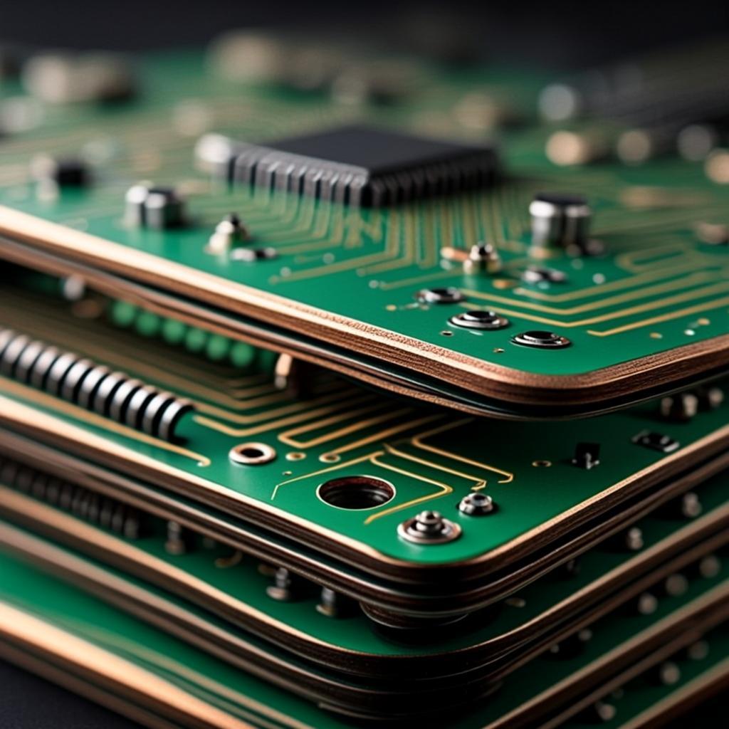
support multilayer printed circuit boards upto 12 layers including impedance control.
Layer-by-layer precision: Our standard file format ensuring seamless 4 and 6-layer PCB designs, ready for accurate fabrication.
Assemble with precision, deliver with confidence. Our PCB assembly services offer tailored solutions for seamless integration.
Our BOM Management Software and Component Procurement Tool are integral parts of our turn-key assembly services. These tools are designed to streamline the process of refining BOMs (Bill of Materials) and efficiently sourcing components for your projects. With our software-driven approach, you can easily optimize your BOMs, identify the right vendors and part numbers, and ensure a smooth ordering process for components. Our goal is to simplify the procurement journey and provide you with a comprehensive solution for managing your assembly requirements.
Selecting 'Automatic Assembly' is a crucial step in choosing the right stencils for your assembly process. Our Automatic Assembly feature ensures compatibility and optimal performance with our SMT stencil options. To guide you through this selection process and ensure seamless integration with our assembly services, we provide comprehensive guidance and support. Explore the benefits of Automatic Assembly and make informed decisions for your projects by following our expert guidance.
When it comes to SMT (Surface Mount Technology) stencil options, we offer a range of choices to meet your specific needs. Our offerings include both frameless and framed stainless steel metal stencils for solder paste application. It's important to note that framed stencils are essential, especially for components like BGA, QFN, or 0402 components, even for prototype quantities. To delve deeper into our SMT stencil options and understand their significance, click the button below to learn more about SMT Stencils.
Upon completion of the PCBA process, we utilize our proprietary machine learning-based Advanced Intelligence-Driven visual inspection system. This system is designed for quality assurance, leveraging AI algorithms to detect defects and anomalies. With each test cycle, the system continuously learns and improves its accuracy, ensuring optimal performance.
In addition to visual inspection, we conduct a range of functional tests to validate the board's performance
Specialised testing for components & batch sizes
Tailored testing solutions to ensure the quality and reliability of your components, regardless of batch size