Learn the complete PCB assembly process flow chart with clear steps, inspection methods, defects, and optimization tips used in modern SMT and THT electronics manufacturing.
Modern electronics rely on accurate PCB assembly (PCBA). A clear PCB assembly process flow chart helps control defects, improve yield, and reduce manufacturing cost, making it essential for hardware designers and anyone sourcing turnkey PCB assembly services.
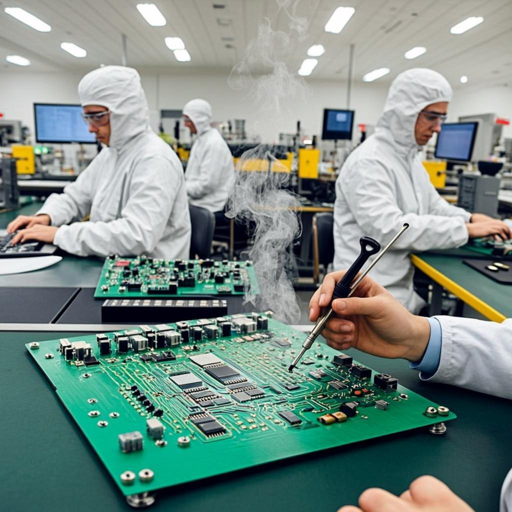
Quick Summary: The PCB assembly process flow chart explains how electronic components are mounted, soldered, inspected, and tested through SMT and THT stages to ensure reliable, defect-free circuit boards in modern electronics manufacturing.
This article is written and verified by Santosh Das, an electronics and technology blogger with over 25 years of real-world experience.
(Conceptual order used in SMT + THT manufacturing lines)
Design Files → Material Preparation → Solder Paste Printing → SPI → Pick & Place → Reflow Soldering → AOI → THT Insertion → Wave/Selective Soldering → Cleaning → Inspection → Functional Testing → Final QC → Packaging
Before production begins, manufacturers verify:
Why important: Early design verification prevents production defects and reduces PCB assembly cost per board.
All components are prepared:
This stage ensures reliable solder joints and improves long-term reliability.
A stainless steel stencil applies solder paste to PCB pads.
Common Defects
Manufacturers use high-precision SMT stencil printers to control paste thickness.
3D SPI machines verify:
This step alone removes nearly 60% of future soldering defects in high-volume electronics manufacturing.
Automated machines mount SMD components at extremely high speed.
Typical placement accuracy: ±30 microns
High-speed machines may place 50,000–120,000 components/hour
The PCB passes through a temperature-controlled oven.
Reflow Profile Stages
Correct temperature profile prevents:
Cameras detect defects such as:
AOI system drastically reduces field failures in contract electronics manufacturing.
Large or mechanical components are inserted:
Can be manual or robotic depending on production volume.
Boards pass over molten solder waves.
Selective soldering is used for mixed SMT-THT boards to protect sensitive SMD components.
Flux residue removed using:
Important for automotive and medical electronics compliance.
Includes:
PCB powered and tested:
Final Quality Check & Packaging of PCB Assembly (Labeling , Anti-static packaging, Moisture barrier bag sealing)