With the rapid advancement of modern electronics, the demand for high-speed, high-frequency PCBs has grown significantly. Devices in industries such as 5G telecommunications, aerospace, radar systems, automotive electronics, and RF communication rely heavily on reliable signal transmission and minimal electromagnetic interference. As a result, engineers must now pay close attention to pcb design rules for high frequency to ensure performance, stability, and compliance.
While high-speed and high-frequency PCBs often overlap in application and design approaches, they are not identical. High-speed PCBs typically focus on fast data transmission rates, while high-frequency PCBs are more concerned with the signal’s operating frequency, especially in the RF and microwave ranges. Nonetheless, both require strict layout considerations, controlled impedance, and careful material selection. Understanding the fundamental differences—and the shared design challenges—is key to creating robust and reliable products that meet today’s performance standards.
Designing high-frequency PCBs comes with several technical challenges that, if not properly addressed, can compromise the performance of the entire system. Strict adherence to pcb design rules for high frequency is essential to ensure reliable signal transmission and electromagnetic compatibility.
One of the most critical concerns is signal integrity (SI). At high frequencies, even small discontinuities in trace layout or layer transitions can cause reflections, ringing, and timing errors. Proper trace routing, impedance matching, and return path planning are vital.
Electromagnetic interference (EMI) and crosstalk also increase with frequency. Uncontrolled energy radiation from traces can affect nearby components or signals, leading to functional failure. pcb design rules for high frequency recommend techniques such as via stitching, controlled trace spacing, and shielding to mitigate these risks.
Another major challenge is impedance control. As signals behave like transmission lines at high frequencies, trace width, dielectric thickness, and PCB material properties significantly impact signal quality.
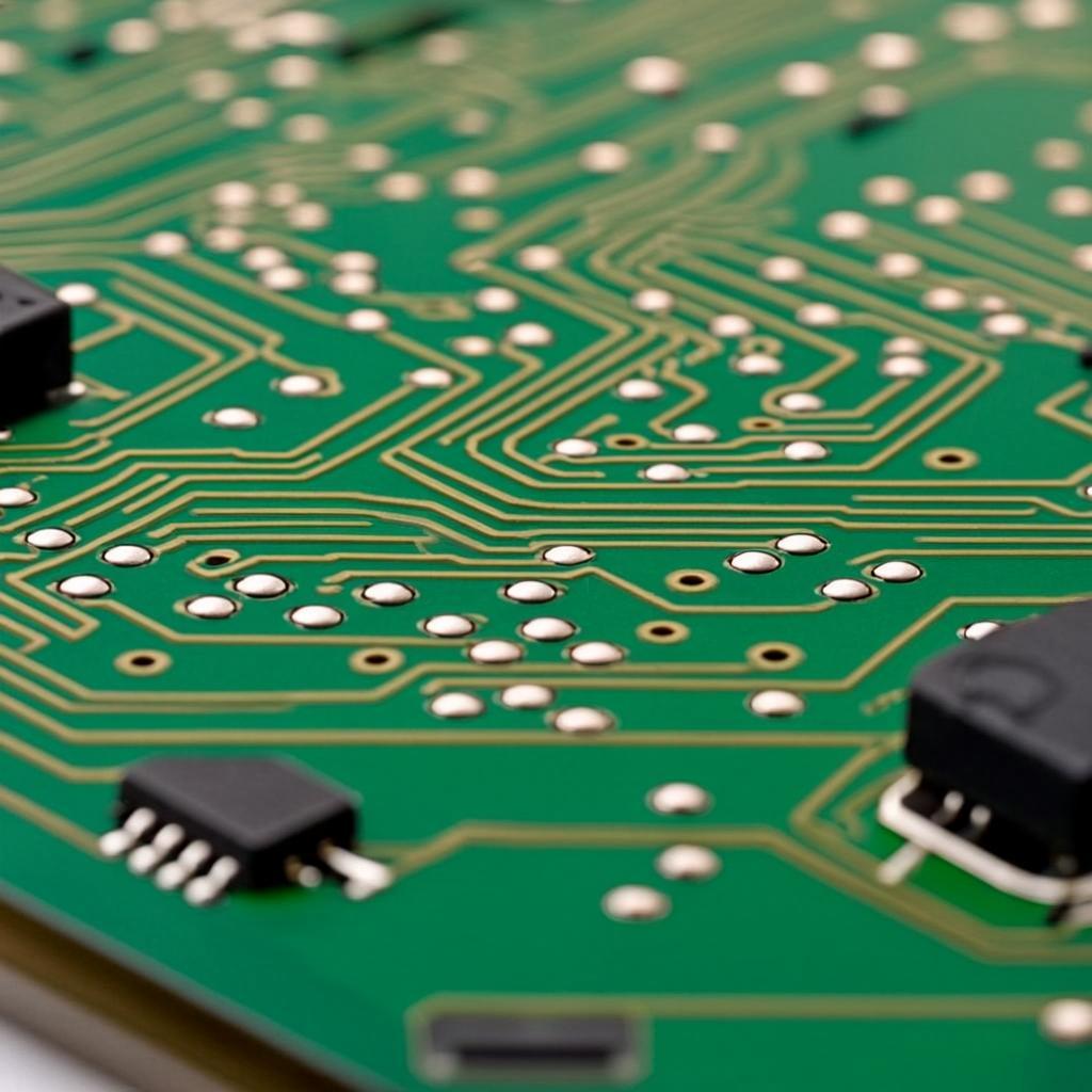
Material selection plays a critical role. Standard FR-4 materials exhibit high loss at GHz frequencies. Designers must choose low-loss substrates like Rogers or Teflon to meet the pcb design rules for high frequency and ensure optimal electrical performance.
To ensure optimal performance and reliability, engineers must follow specific pcb design rules for high frequency. These guidelines address the physical and electrical constraints that come into play when dealing with GHz-level signals and fast edge rates. Below are the key design principles every high-frequency PCB layout should consider.
A well-structured layer stack-up is foundational to effective high-frequency design. Multilayer PCBs allow better signal referencing and shorter return paths, both critical to minimizing EMI. According to pcb design rules for high frequency, placing ground and power planes close to signal layers ensures stable impedance and reduces noise coupling. Symmetrical stack-ups are also recommended to prevent board warpage during manufacturing and thermal cycling.
At high frequencies, transmission line effects dominate, making impedance control essential. Impedance is influenced by trace width, dielectric height, copper thickness, and the substrate’s dielectric constant (Dk). Precise impedance matching reduces signal reflections and maintains integrity. Using impedance calculators and signal integrity simulation tools during the layout phase helps predict and optimize performance.
Efficient trace routing directly impacts high-frequency behavior. Routing should be as short and direct as possible, with minimal stubs or sharp angles. 90° trace corners can cause signal reflections and should be replaced with 45° bends or smooth arcs. For differential pairs, match trace lengths and spacing to maintain consistent impedance. Minimizing vias is another essential tip in pcb design rules for high frequency, though when necessary, stitching vias should be used to maintain solid return paths.
Solid ground planes are vital for high-frequency return paths and signal referencing. Discontinuities in ground can lead to impedance breaks and EMI issues. The pcb design rules for high frequency emphasize the importance of reducing ground loop areas and maintaining a continuous plane beneath signal traces. Decoupling capacitors should be placed close to power pins to filter noise and stabilize voltage levels.
Controlling electromagnetic interference is one of the top priorities in high-frequency PCB design. Via stitching around sensitive zones or along the board edge can help contain radiation. Shielding critical components and isolating analog and digital domains are recommended practices. Furthermore, keeping high-frequency traces away from board edges reduces unintended emissions.
To effectively manage electromagnetic performance and signal integrity, designers must apply specific layout rules that are foundational to pcb design rules for high frequency. These rules help control crosstalk, reduce electromagnetic radiation, and ensure a stable operating environment for high-speed signals.
A critical principle in high-frequency PCB design, the 20H Rule is used to minimize power plane radiation. This rule recommends that the power plane be inset from the ground plane edge by a distance equal to 20 times the dielectric thickness (H) between them. The idea is that this offset causes the fringing electric field at the edge of the power plane to cancel out, thereby reducing EMI emissions.
Practical Example:
If the dielectric between the power and ground planes is 0.25 mm, then the power plane should be shrunk inward by 5 mm (20 × 0.25 mm) relative to the ground plane. This technique is especially effective in multilayer boards used in RF, aerospace, or automotive designs where EMI compliance is critical.
Both the 3W and 3H Rules are vital components of pcb design rules for high frequency, aimed at reducing signal coupling and mutual interference between traces.
Use Case Example:
In high-speed communication boards (e.g., SerDes or DDR routing), applying the 3W Rule can significantly reduce near-end and far-end crosstalk, while the 3H Rule ensures vertical layer isolation in complex stack-ups.
By incorporating these rules early in the layout process, designers can meet stringent design standards for high-frequency applications and improve overall signal fidelity and system reliability.
Choosing the right PCB substrate material is fundamental to meeting the pcb design rules for high frequency, as material properties directly affect signal loss, impedance, and overall signal fidelity. At GHz-level frequencies, even minor dielectric inconsistencies can lead to significant performance degradation.
While FR-4 is widely used for general-purpose PCBs, it has major limitations when applied to high-frequency applications. Its relatively high Dk (Dielectric Constant) variation and high Df (Dissipation Factor) lead to increased signal attenuation, especially above 1 GHz. These losses manifest as reduced signal amplitude, higher jitter, and potential timing errors — all of which compromise signal integrity and overall performance.
To overcome these challenges, it is recommended to use advanced materials specifically engineered for RF and microwave circuits. Some commonly used high-performance substrates include: