Multilayer PCB production sits at the core of modern electronics. You see it when space is tight and signals move fast. As layer count rises, control matters more. Small choices early affect yield, noise, and long-term reliability.
Multilayer PCBs are printed circuit boards with more than two copper layers. You usually see 4, 6, or 8 layers. High-end designs can reach 48 layers. Each copper layer sits between insulating materials. This stack lets you route more signals in less space. That matters in phones, medical tools, and car systems. Signals run cleaner, even above 10 GHz. Dedicated power and ground planes also cut noise. EMC improves as a result. When you understand multilayer PCB production, you gain control over size, speed, and reliability.
You begin with careful file review. Stack-up details, trace width, spacing, and impedance all get checked. DFM rules guide these decisions. Gerber files then define every layer. This stage sets limits and expectations. It saves time, material, and frustration later.
Inner layers carry most signal routing. Copper panels get coated, exposed, and etched. Traces must stay sharp and consistent. AOI follows right away. Finding defects here protects the entire panel from scrap.
Finished inner layers are stacked with prepreg insulation. Heat and pressure bond them into one solid panel. Resin flow must stay controlled. Too much or too little causes gaps or shifts. This step defines board strength and layer position.
Drilling creates electrical paths between layers. These holes become vias. Accuracy matters at very small scales. Blind and buried vias need extra care. Clean hole walls are critical for later plating.
Plating starts inside the vias. Thin copper forms first, then thickness builds up. This step connects all layers electrically. Uniform plating matters. Weak spots cause failures under heat or stress.
Outer layers form the visible circuitry. Imaging and etching repeat here. Registration must stay tight. At this point, defects are easier to see and harder to fix. Control stays strict.
Solder mask protects copper and controls solder flow. It covers traces but leaves pads open. Registration matters a lot. Poor mask work leads to shorts, bridges, and rework during assembly.
Silkscreen adds reference marks and labels. It guides assembly and inspection. Clear text helps technicians work faster. Accuracy matters more than appearance.
Surface finish protects copper pads from oxidation. It also improves solder wetting. HASL, ENIG, and OSP are common options. The right choice depends on assembly method and reliability needs.
Profiling separates boards from the panel. Routing or V-scoring defines final shape. Clean edges reduce cracking and handling damage. Proper profiling improves fit in enclosures.
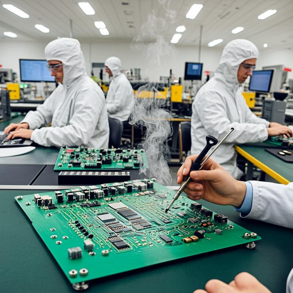
Quality checks run throughout production. AOI, electrical testing, and visual inspection work together. You verify continuity and isolation. Consistent inspection protects long-term performance.
Finished boards require careful handling. Moisture and static are constant risks. Dry packing and ESD protection are essential. Even high-quality boards suffer if packaging fails.
Multilayer PCBs bring strong benefits when space and performance matter. You pack more function into a smaller area. Electrical behavior improves as well. These advantages explain why multilayer boards dominate modern electronics.
Multilayer PCBs also bring trade-offs. You gain performance, but complexity rises. These limits matter during planning and budgeting.
Testing confirms that a multilayer PCB works as designed. You verify electrical paths, component behavior, and visual quality. As layer count increases, risk increases too. Testing reduces that risk before boards reach assembly or field use.
ICT checks each node on the board. It finds shorts, opens, and wrong component values. A fixture contacts many points at once. This test is fast and repeatable for volume builds.
Functional testing powers the board. You check how it behaves in real conditions. Signals, timing, and outputs get verified. This step confirms the board actually does its job.
Flying probe testing uses moving probes instead of fixtures. It suits prototypes and small batches. Setup is quick. Test speed is slower, but flexibility is high.
AOI scans the board visually. It detects misalignment, opens, and solder issues. Cameras compare results to reference data. This catches defects the eye might miss.
For high-speed boards, extra checks apply. Signal paths get reviewed for impedance and crosstalk. Values must stay within tight limits, often around ±10% of target impedance. Testing is not optional. It protects reliability and performance in multilayer PCB production.
Multilayer PCB production brings real technical pressure. Layer stacking must stay accurate. Small shifts during lamination can disturb signal paths. Drilling errors can break vias and cut connections. These risks grow fast beyond twelve layers.
Thermal behavior adds another challenge. Materials expand at different rates. Even a small mismatch can warp the board. High-speed designs raise the bar further. Impedance must stay controlled. Crosstalk must stay low. You balance cost, process limits, and performance at every step.
Electronics keep getting smaller. This drives the use of HDI in multilayer PCB production. You place more routing in less space. Fine traces and tight spacing support dense components. Standard vias no longer fit modern layouts.
HDI uses very small line width and spacing. Values often reach 3 mil or below. This allows routing under fine-pitch BGAs. Signal paths stay short. Density increases without adding more layers.
Blind vias connect outer layers to inner layers. They stop before reaching the bottom. Buried vias connect only internal layers. Both save surface space. They also increase process steps and control needs
Microvias stay small in diameter, often 0.15 mm or less. Laser drilling forms them with precise depth control. You use microvias to escape dense IC pads. Routing remains clean and controlled.
Microvias have tight depth-to-diameter limits. Copper must plate evenly. Poor plating causes weak connections. Staggered microvias reduce stress compared to stacked designs.
Via-in-pad places a microvia inside a component pad. Trace length drops. Signal quality improves. Modern solid-plated microvias remove extra filling steps. This keeps cost and risk lower.
HDI boards require multiple lamination cycles. Each cycle adds drilling and plating. Alignment must stay exact. This raises lead time and cost. The reward is higher density in fewer layers.
HDI changes how multilayer boards are built. Control replaces tolerance. Precision replaces margin. When executed well, HDI enables compact, high-performance designs that standard boards cannot support.
As a leading manufacturer in multilayer PCB production, PCBMay focuses on producing high-performance PCBs with up to 40 layers. We offer rich and extensive experience in advanced technologies such as HDI, high-frequency/high-speed, and microwave PCBs.
Based on your project requirements, we can also use premium substrate materials like Rogers, Taconic, and Isola. These are suitable for demanding applications including 5G base stations, aerospace systems, and industrial radar equipment.