In the era of intelligent living, smart homes are no longer futuristic concepts—they are practical ecosystems built upon seamless electronic integration. At the foundation of every smart device lies a Printed Circuit Board Assembly (PCBA), the vital component that connects sensors, processors, and communication systems into one coherent network.
Smart Home PCB Assembly refers to the engineering and manufacturing process that transforms a bare circuit design into a fully functional module capable of managing automation, sensing, and data communication across an entire household. It is the invisible architecture that enables homes to think, respond, and adapt.
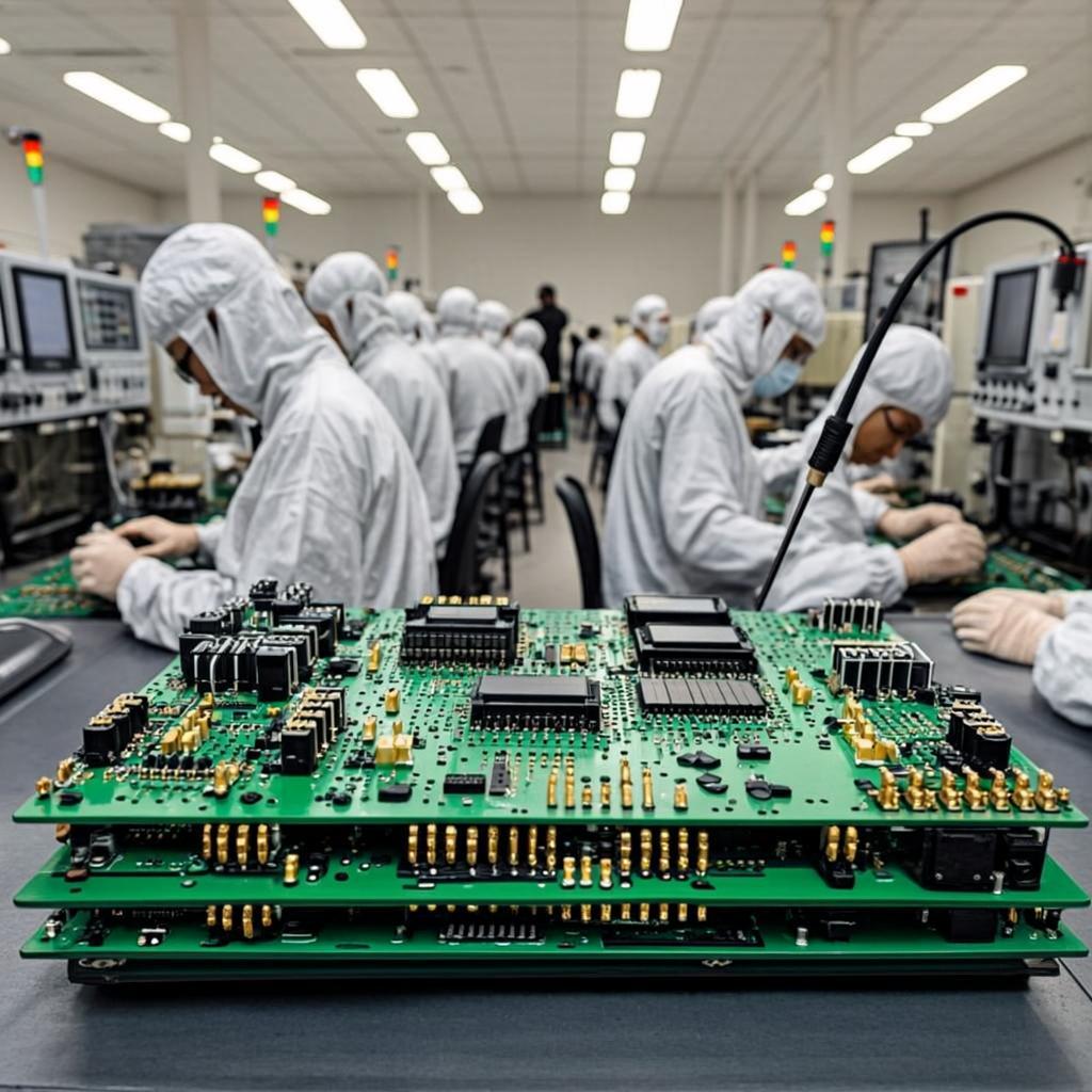
Smart home PCB assemblies are not just electronic boards—they are multi-layered systems integrating signal processing, communication control, and power optimization.
Each PCB must balance electrical performance, thermal management, and EMC (Electromagnetic Compatibility) to ensure stable and interference-free operation.
Engineers select high-Tg FR4, Rogers, or metal-based substrates depending on thermal requirements and circuit density. Surface Mount Technology (SMT) and Through-Hole Assembly (THA) techniques are applied to mount components such as microcontrollers, communication modules, and power ICs with precision. This ensures compact layouts, reduced noise, and high reliability under 24/7 operation.
A modern smart home PCB typically integrates several critical modules that define its performance:
Depending on application scenarios, PCB assemblies can take many specialized forms:
Each design demands specific PCB stack-ups, controlled impedance routing, and EMI shielding to ensure performance consistency across environments.
Smart home devices operate continuously, often in variable conditions. Therefore, reliability is non-negotiable.
During assembly, strict process control is applied to reflow soldering, X-ray inspection, and AOI (Automated Optical Inspection). Functional testing ensures every PCBA meets design specifications before integration into final products.
KKPCB emphasizes IPC-A-610 Class 2/3 compliance, RoHS and REACH environmental standards, and advanced DFM (Design for Manufacturability) review during the prototyping stage to minimize risk and enhance performance consistency.
At KKPCB, we combine engineering precision, manufacturing expertise, and reliable supply chain management to deliver Smart Home PCB Assemblies that meet global standards.
Our services cover schematic design, PCB layout, component sourcing, SMT assembly, functional testing, and mass production, ensuring one-stop delivery from concept to reality.
With our expertise, clients can accelerate time-to-market, enhance product quality, and innovate confidently within the fast-evolving smart home industry.