Taconic PCBs are one of the leading materials for performance-oriented electrical components like Printed Circuit Boards (PCBs). As the name suggests, Taconic PCBs are rooted in a famous manufacturing brand in the US- Taconic. They are known for a wide set of unique properties, which makes them suitable for various industries like defence, communication, healthcare, etc.
This blog will give a comprehensive overview of Taconic PCBs, including what it is, their benefits, specifications, applications, and design techniques.
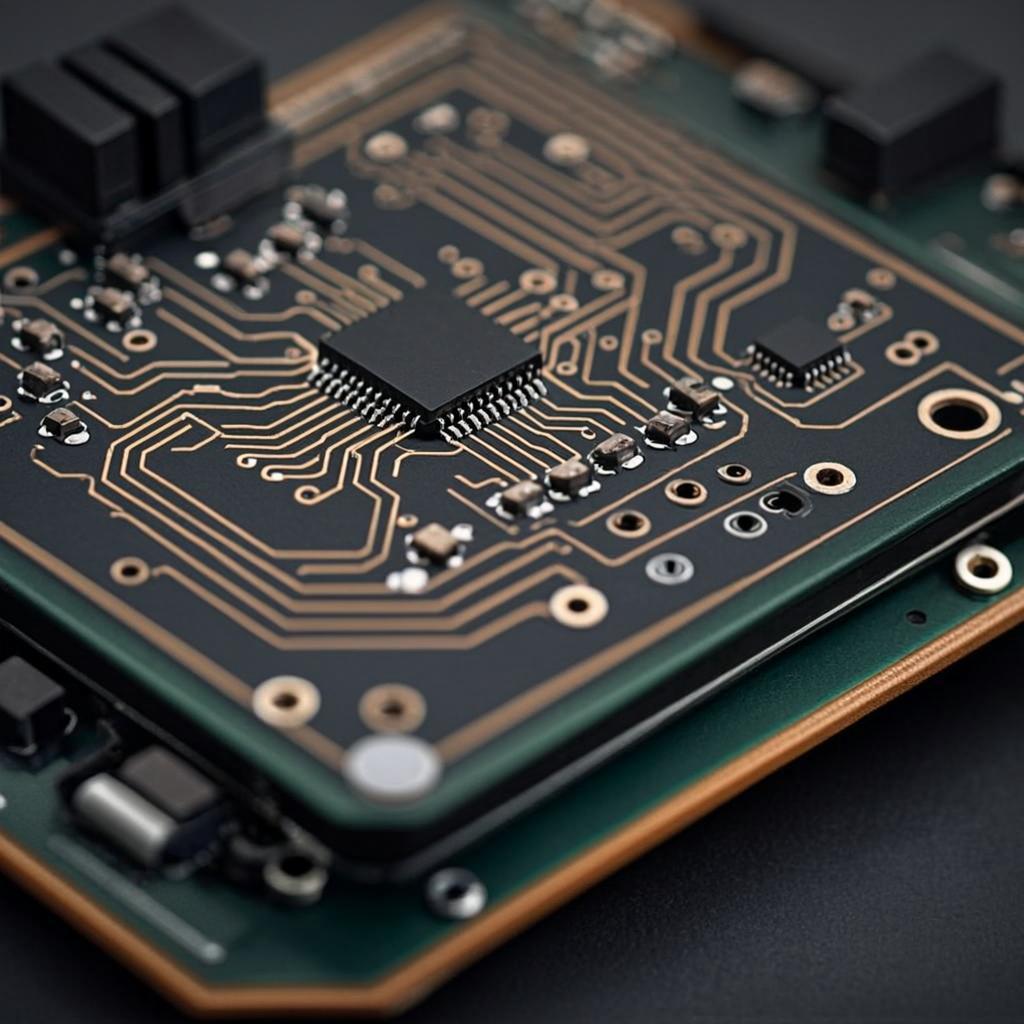
Taconic PCBs are high-frequency boards created through the components manufactured by Tacon, a leading material manufacturer. It is their unique composition mix that makes them stand out from the market alternatives. They are mainly composed of PTFE (polytetrafluoroethylene) and ceramic-filled substrates.
Such a combination ensures dielectric constant stability for quicker transmission of signals. Similarly, Taconic PCBs exhibit excellent thermal management, which helps the PCB components to withstand the pressure from harsh environments.
Several stages are involved in the manufacturing process of Taconic PCBs. Have a look at them:
Raw materials play an important role in ensuring the quality of the Taconic PCB. Therefore, set up a team of expert professionals to choose the best PTFE materials. High-quality ceramic-filled PTFE components ensure higher thermal conductivity and help the components withstand harsh chemicals like aqua regia. These PTFE matrices, ceramic fillers, and reinforcing fabric are combined to create a high-performance laminate material.
After cleaning the surface, a photosensitive film is applied to the surface. As the next step, a photomask is used to expose the photoresist to UV light, which hardens the exposed areas. Now, simply wash away the remaining photoresist material and unexposed spots to get the desired circuit pattern. If needed, use a chemical solution for PCB etching to wipe out the unwanted copper.
Drill precise holes into the PCB surface with reference to the design in order to create vias for component mounting. After drilling, plate the holes with a thin layer of copper to connect multiple layers of the board.
Now it's time to coat the PCB with epoxy solder mask ink on both sides. This is mainly done to protect the copper layer. The portions with solder mask coating are exposed to UV light to harden the spots. Just like photolithography, clean away the unexposed parts and bake them with an oven to harden the solder mask even further.
Manufacturers are required to try out both visual inspections and automated optical inspections (AOI) to detect any faults in the Taconic boards. Once the experts raise the green flag, it is moved to PCB assembly.
Taconic PCBs often remain the top choice for manufacturers due to a wide range of benefits. Check out them:
The advanced component composition of Taconic PCBs, including thermoset resins and ceramic fillers, equips them with superior dielectric properties. As a result, electronic devices, especially communicative systems, can work with faster signal transmission.
Luckily, Taconic PCBs help devices withstand harsh environmental conditions without any performance degradation. As a result, the lifetime of devices may increase.
The low dielectric constant is one of the most highlighted properties of Taconic PCBs. It keeps the energy loss during signal transmission to a minimum. Therefore, Taconic PCBs are an apt choice for devices like radar systems that demand signal strength.
As compared to other PCBs, Taconic PCBs have excellent thermal management capabilities which makes the PCB components endure higher temperature processes without any issues. It is particularly useful for high-frequency PCB applications where overheating is a serious concern.
What makes Taconic PCBs stand out in the market is their unique properties. Here are some of them:
Taconic PCBs have a wide range of applications across many industries. Here's a brief overview of how it is used:
Taconic materials are mainly used in RF PCBs and microwave circuits due to their low dielectric constant which improves signal strength. That's why many communication devices like antennae, transmitters, receivers, etc., use them.
The mechanical strength of Taconic PCBs prepares device components to work under harsh conditions. Therefore, it is highly useful in devices like a radar system, missile guidance systems, satellite communicators, etc.
The high level of precision of Taconic PCBs makes it a better choice for diagnostic equipment like medical scanners that require advanced imaging.
Taconic PCBs are increasing their presence in the automotive sector, especially in Advanced Driver-Assistance Systems (ADAS). Some of the common applications are:
To have a better overview, let's have a competitive analysis of Taconic PCB and Isola PCB, a high-performance board created using laminated materials.
Even though both Taconic and Isola PCBs are known for less dielectric constant, Taconic has a relatively much lower figure, starting from just 2.17. Moreover, the dissipation factor of Taconic PCBs is also lower (0.0009 at 10 GHz).
Taconic PCBs demonstrate higher thermal stability with decomposition temperatures up to 526°C which is higher than the Td values of Isola which is just 360°C. That means Taconic PCBs are a better choice for electrical devices requiring high-temperature operations.
Both Taconic and Isola PCBs are used in high-frequency devices due to the low dielectric constant and dissipation factor. However, Isola may have more energy loss at higher frequencies.
Isola laminates are readily available in the markets and are less costly as compared to Taconic materials, making them perfect for manufacturers working under a tight budget.
Taconic PCBs are preferred for high-frequency applications in various industries like medical, communication, aerospace, defence, etc., where signal strength is a crucial factor. But Isola PCBs are more used in high-speed RF and microwave circuits.
Check out the most common types used Taconic PCB laminates and their key properties:
They are ceramic PCB-filled PTFE-based laminate reinforced with woven glass and are known for excellent thermal stability with a decomposition temperature of up to 420°C. Therefore, they are more suitable for high-performance RF and microwave applications.
It has the lowest dielectric constant and dissipation, which cuts down signal loss during transmission.
Taconic CER-10 has the highest dielectric constant of about 10. That's why it is mainly used in devices like power amplifiers and filters that require high thermal management capabilities.
It is a dimensionally stable, low-loss laminate material from Taconic. Just like Taconic TLY-5, it is specialised in improving signal strength and is therefore used in communicative devices such as radar, satellite systems, etc.
The selection of a Taconic laminate purely depends on your requirements since each type has its own properties. For instance, Taconic RF-35 and TLY-5 are preferred for low-loss applications, while CER-10 is suitable for high-power applications. If you want to have a balanced approach from both performance and cost angles, TSM-DS3 might be the perfect choice.
While manufacturing Taconic PCBs, each step of the manufacturing must be done in the presence of experienced professionals to avoid any kind of issues. Here are some technical guidelines for the process:
At high frequencies, the electromagnetic fields around traces can crosstalk between adjacent signals. To avoid this, place the traces in wider spaces. Similarly, optimise the vias and layer transitions to improve the overall signal quality.
Place the reference planes and control the dielectric thickness to attain the target 50Ω impedance. Manufacturers can use 2D and 3D field solvers to model the impedance of complex PCB layers structures accurately.
Ensure proper airflow around heat-generating components for effective thermal management. And, consider using thermal vias to connect the top copper layer (where the heat-generating components are located) to the ground plane for easy transfer of heat. The usage of thermal relief pads can reduce stress.
Use EM simulation tools to optimise the PCB layout design and identify any issues earlier. Similarly, conduct thermal simulations to make sure that the Taconic PCB can operate within safe temperature limits.
As the demand for Taconic PCBs is increasing in a fast-paced manner, its presence is expanding to many industries like wearables, healthcare, etc. Its unique properties like low dielectric constant and dissipation factor make it capable enough to support next-generation technologies like 5G and millimetre wave. Overall, the future trends are tilting in favour of a wide-scale adoption of Taconic PCBs.