Helen Frankenthaler PCB Circuit Board R&D Center

Taconic Prototype PCB for Communication Equipment

Ceramic PCB - LSTPCB

Ceramic PCB

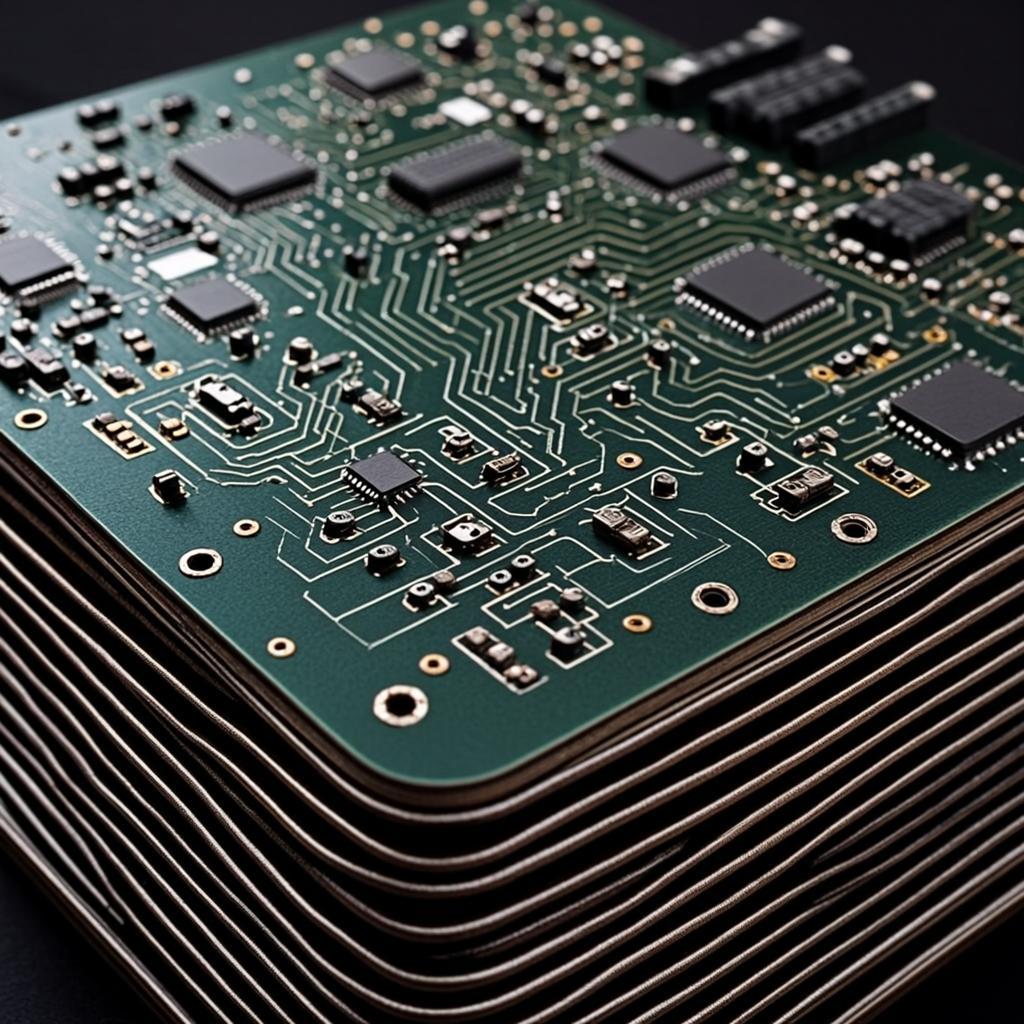
Ceramic PCB is a circuit board made by using ceramic material as the substrate and bonding copper foil directly to the surface of the ceramic substrate through a special process.

PRODUCTS

  • Ceramic PCB
  • high frequency PCB
  • Rigid and flexible pcb
  • IC Substrate
  • OEM/ODM Products
  • Medical PCB
  • Consumer Electronics PCB
  • Smart PCB
  • Industrial PCB
  • New Energy PCB
  • IOT PCB

Ceramic PCB

AMB Ceramic Copper-Clad Substrate
DPC Aluminum Oxide Double-Sided ENIG/Silver Ceramic Substrate
Direct Bonded Copper Ceramic PCB
Direct plating copper ceramic PCB

Introduction to Ceramic PCBs

Ceramic Printed Circuit Boards (Ceramic PCBs) are a specialized type of circuit board that use ceramic materials as the substrate, such as alumina, aluminum nitride, and beryllium oxide. These high thermal conductivity materials can rapidly transfer heat away from hotspots and dissipate it evenly across the surface. Additionally, ceramic PCBs are manufactured using LAM (Laser Rapid Activation Metallization) technology, which ensures precise and efficient metallization. Owing to their exceptional thermal conductivity, high-temperature resistance, and stability, ceramic PCBs are widely used in high-power, high-frequency, and high-temperature electronic devices.

Characteristics of Ceramic PCBs
  • Thermal Conductivity: Ceramic materials such as alumina (Al₂O₃) and aluminum nitride (AlN) possess excellent thermal conductivity, effectively transferring heat to heat sinks or dissipators. This significantly enhances heat dissipation, which is crucial for high-power electronic devices.
  • Electrical Performance: Ceramic materials have a low dielectric constant and dielectric loss, reducing energy loss and signal distortion during transmission. Additionally, ceramic PCBs offer superior insulation properties, effectively preventing crosstalk and interference between circuit layers.
  • Mechanical Properties: Ceramic PCBs feature high hardness and strength, allowing them to withstand external impacts and vibrations, thereby enhancing shock resistance. Moreover, ceramic materials exhibit excellent corrosion resistance and high-temperature stability, making them suitable for harsh operating environments.
  • Dimensional Stability: The thermal expansion coefficient of ceramic materials closely matches that of silicon chips, resulting in minimal dimensional changes under high temperatures. This ensures the stability and reliability of the circuit board.

Ceramic PCB

Types of Ceramic PCBs
  • Single-Layer Ceramic PCB: Features a single conductive layer on a ceramic substrate.
  • Multi-Layer Ceramic PCB: Composed of multiple ceramic substrates with conductive traces and vias connecting different layers, suitable for complex circuit designs, high-density interconnections, and applications requiring signal integrity.
  • Thick-Film Ceramic PCB: Utilizes thick-film technology to create conductive and resistive traces on the ceramic substrate.
  • Thin-Film Ceramic PCB: Involves depositing thin layers of conductive and insulating materials onto the ceramic substrate, providing precise electrical characteristics, typically used in high-frequency applications such as RF and microwave devices.
  • Hybrid Ceramic PCB: Combines ceramic materials with other substrates, such as organic or metal-core materials, to balance the advantages of ceramics with those of other materials.
Our capabilities
Process parameters
contentProcess parameters
Substrate Typeconventional Alumina 96%; Alumina 99% Aluminum nitride (≥170 W/MK), aluminum nitride (≥230 W/MK) Customizable Silicon carbide, silicon nitride, zirconium oxide, ZTA, diamond, sapphire, polycrystalline silicon wafer
Substrate specificationsthickness 0.1—3.0mm, customized is accepted Length and width Regular size 120*120mm, custom sizes accepted
Number of layers Line layersSingle-sided, double-sided
Copper coating processDPC/DBC
hole shapeRound holes, square holes, special-shaped holes, countersunk holes, and sinks
ApertureMin. 0.05mm
Aperture tolerance+/-0.025mm
Hole MetallizationCan be metallized and plated to fill holes
Aspect Ratio1:10
Side metallizationHalf hole process and side edge metallization are possible
lineCopper thickness 1–1000um, customized is accepted Dam–1500um Minimum line width 0.05mm Minimum spacing 0.05mm Layer bias+/-5um
testElectrical performance test Open and short circuit test, impedance test, special test, flying probe test
Process parameters
contentProcess parameters
Solder Mask Ink BrandSun PSR2000/4000 Series
colorGreen, white, black, blue, customizable
Minimum oil bridge0.1mm
character colorWhite and black are available for customization
Minimum character width0.1mm
Minimum character height0.7mm
Surface treatmentSilver Ag—0.4-0.9um Immersion Nickel Gold Ni: 3–7um, Au: 0.025–3um Nickel Palladium Gold Ni: 3–7um, Pd: 0.025–0.075um Au: 0.025–3um other OSP 0.2-0.5um, blue glue, carbon oil
shape Shipping methodLaser cutting/water jet cutting/single piece/pre-cutting/no pre-cutting
Minimum unit size1 X 1 MM
Finished product shapeSquare, round, special shape
Dimensional toleranceNormal +/-0.1mm, special requirements: +/-0.02mm

Follow Us