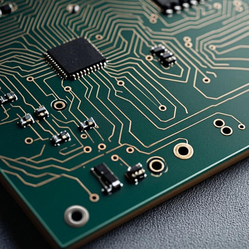
In the world of IoT product development, the printed circuit board (PCB) is more than just a substrate for components—it’s the physical manifestation of your entire system architecture. A well-designed PCB directly determines whether your IoT device will function reliably in diverse environments, meet regulatory requirements, achieve promised battery life, and scale cost-effectively to production.
Consider this: approximately 40% of IoT product failures trace back to PCB design issues—unexpected power consumption, electromagnetic interference, manufacturing defects, or environmental vulnerabilities. The difference between a prototype that works on your desk and a production-ready product lies in how you approach PCB design from day one.
Prototype PCBs are about proving functionality: can we make it work once?
Production PCBs are about ensuring reliability: will it work consistently for thousands of devices across different environments while meeting cost targets and certification requirements?
This article focuses on bridging that gap, providing practical PCB design fundamentals specifically for IoT product developers who need to move from concept to scalable product.