Helen Frankenthaler PCB Circuit Board R&D Center

Teflon Flex PCB for Smart Home

Teflon PCB Manufacturer | High-Frequency PTFE PCB Solutions for Extreme Environments - HCJMPCBA

Teflon PCB Manufacturer

High-Frequency PTFE PCB Solutions for Extreme Environments by HCJMPCBA

1. Introduction to Teflon PCB

A Teflon PCB (or PTFE PCB) is a printed circuit board fabricated using polytetrafluoroethylene (PTFE)—a high-performance polymer renowned for its exceptional electrical, thermal, and chemical properties. As a material, PTFE (commercially known as Teflon) delivers:

  • Ultra-low dielectric loss for high-frequency signal integrity.
  • Extreme temperature resilience (-200°C to 260°C continuous operation).
  • Chemical inertness against acids, bases, and solvents.

These attributes make high frequency Teflon PCBs indispensable for applications like 5G infrastructure, aerospace sensors, medical devices, and industrial RF systems—where traditional FR4 substrates fail to meet performance or environmental demands.

2. Core Advantages of Teflon PCB

The technical superiority of Teflon PCBs stems from PTFE’s material science. Below is a data-driven breakdown of their key benefits:

AdvantageTechnical SpecificationBusiness Impact
Ultra-Low Dielectric LossDF ≤ 0.001 @ 10GHz (varies by PTFE grade)Enables 5G/6G mmWave (28–77GHz) and satellite communications with minimal signal attenuation.
Stable Dielectric ConstantDK = 2.1–2.3 (deviation ±0.02 across temperature/frequency)Ensures consistent impedance control (50Ω/75Ω) for high-speed digital and RF designs.
Extreme Temperature Tolerance-200°C to 260°C continuous operation; short-term up to 300°CSuitable for aerospace (cryogenic environments) and medical (autoclave sterilization) applications.
Ultra-Low Moisture AbsorptionMoisture absorption < 0.01% (compliant with IPC-4101 Class H)Guarantees long-term reliability in humid or outdoor environments (e.g., 5G base stations).
Chemical InertnessResistant to acids, bases, solvents, and most industrial chemicalsIdeal for industrial sensors and marine electronics exposed to corrosive substances.

3. Teflon PCB Material Types & Specifications

PTFE-based laminates vary by filler, thickness, and performance. Below is a comparison of mainstream Teflon PCB materials:

PTFE GradeDielectric Constant (DK) @ 10GHzDielectric Loss (DF) @ 10GHzThickness Range (mm)Key FeaturesTypical Applications
Dupont Teflon™ AF2.1 ± 0.020.00090.025–1.5Fluorinated ethylene propylene (FEP) filler, ultra-low loss, flexible60GHz mmWave antennas, high-speed digital backplanes
Dupont Teflon™ F4B2.2 ± 0.020.0010.1–3.0Glass fiber reinforcement, rigid, cost-effective5G base station RF modules, automotive radar
Domestic Modified PTFE (HCJMPCBA Custom Grade)2.2 ± 0.030.0010.1–2.0Ceramic filler, 30% cost reduction vs. imported gradesIndustrial RF sensors, mid-range wireless systems

4. Teflon PCB Manufacturing Process

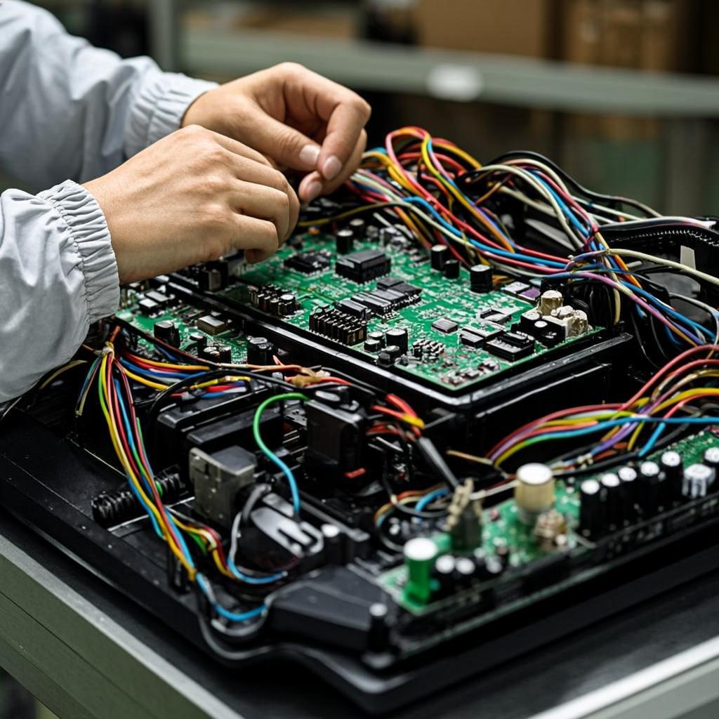
Fabricating Teflon PCBs requires specialized equipment and strict process control. Here’s a detailed breakdown:

Step 1: Lamination
  • Parameters:
    • Temperature: 300–380°C (varies by PTFE grade; e.g., Teflon™ AF requires 350°C).
    • Pressure: 50–100 bar.
    • Hold Time: 60–120 minutes to ensure complete curing and void-free bonding.
  • Challenge: Maintaining uniform pressure across the panel to prevent delamination, especially for multi-layer stacks.
Step 2: Drilling
  • Methods:
    • Laser Drilling: Minimum hole diameter 0.1mm, positional accuracy ±0.01mm, hole wall roughness Ra ≤ 0.5μm.
    • Mechanical Drilling: For larger holes (≥0.3mm), using carbide drills with TiAlN coating to withstand PTFE’s abrasiveness.
  • Inspection: Post-drilling AOI (Automated Optical Inspection) to verify hole size, location, and absence of debris.
Step 3: Plating & Surface Finish
  • Plating: Copper thickness 1–3oz, with electroplating current density 2–4 A/dm² for uniform coverage.
  • Surface Finish Options:
    • ENIG (Electroless Nickel Immersion Gold): ≥0.05μm gold thickness for wire bonding and high-reliability applications.
    • Hard Gold Plating: 0.5–2.0μm gold thickness for wear-resistant contacts (e.g., switches, connectors).
    • OSP (Organic Solderability Preservative): Cost-effective for short-term storage in controlled environments.
Step 4: Testing & Validation
  • Electrical Testing: TDR (Time Domain Reflectometry) for impedance control (±5% tolerance) and flying probe for 100% continuity.
  • Thermal Testing: Thermal cycling (-200°C to +260°C, 500 cycles) to validate long-term reliability.
  • X-Ray Inspection: Verifies via integrity and copper thickness uniformity.

5. Application Cases (Industry-Specific)

Teflon PCBs enable innovation in industries with extreme performance demands:

5G & mmWave Communications
  • Solution: Teflon™ AF PCB (DK=2.1, DF=0.0009) for 77GHz automotive radar modules.
  • Outcome: Supports 77GHz frequency band with 40% lower signal loss than FR4, enabling 300m detection range for autonomous vehicles.
Medical Devices
  • Solution: Teflon™ F4B PCB for autoclave-sterilized surgical tools.
  • Outcome: Withstands 260°C steam sterilization cycles, meets ISO 10993 biocompatibility standards, and maintains electrical performance over 5,000 sterilization cycles.
Aerospace & Defense
  • Solution: Custom modified PTFE PCB for satellite payloads.
  • Outcome: Operates in -200°C cryogenic environments with dimensional stability ≤0.05%, ensuring 10-year mission reliability.
Industrial RF Systems
  • Solution: Domestic modified PTFE PCB for industrial IoT sensors.
  • Outcome: Resists harsh chemicals (acids, solvents) in manufacturing plants, with a 50% longer lifespan than FR4-based sensors.

6. Teflon PCB Design Guidelines: HCJMPCBA’s Expert Checklist

To maximize performance and manufacturability, follow these guidelines:

Design AspectBest PracticeRationale
Impedance ControlTarget 50Ω (single-ended) / 100Ω (differential), account for DK deviation ±0.02Ensures signal integrity for RF and high-speed digital applications.
Trace RoutingTrace width ≥0.15mm, spacing ≥0.15mm; use curved traces (avoid 90° bends)Minimizes signal reflection and crosstalk in high-frequency designs.
Thermal ManagementPlace 2–3 thermal vias (0.3mm diameter, copper-filled) per cm² under power componentsEfficiently dissipates heat, preventing component overheating in high-power RF modules.
Mechanical ReliabilityMaintain ≥0.5mm copper edge clearance; use stiffeners for flexible PTFE gradesPrevents copper cracking and board warpage during assembly and operation.

7. HCJMPCBA’s Teflon PCB Manufacturing Capabilities

As a leading Teflon PCB manufacturer, HCJMPCBA delivers industry-leading precision and flexibility:

CapabilityTechnical SpecificationBusiness Benefit
Material CoverageDupont Teflon™ AF, F4B, and domestic modified PTFE gradesSupports diverse applications from 5G to aerospace.
Manufacturing PrecisionLayer alignment tolerance ±0.02mm, impedance control ±5%Ensures consistent signal integrity for high-frequency designs.
Quality CertificationsISO 9001, AS9100 (aerospace), ISO 13485 (medical), RoHSQualifies for regulated industries (automotive, medical, aerospace).
Turnaround TimePrototypes: 3–5 days; Mass production: 7–10 daysAccelerates product development cycles.
Global Sourcing & DeliveryDirect sourcing from Dupont and domestic suppliers; delivery to North America, Europe, AsiaMinimizes lead time and supports global supply chains.

8. In-Depth FAQs About Teflon PCB

1. How to select the right PTFE laminate for 77GHz automotive radar?

For 77GHz, prioritize Dupont Teflon™ AF (DK=2.1, DF=0.0009) due to its ultra-low loss and FEP filler, which minimizes signal attenuation in mmWave bands. Ensure the laminate thickness (e.g., 0.127mm) aligns with your impedance and mechanical requirements.

2. What are the common defects in Teflon PCB lamination and how to solve them?

Delamination: Caused by insufficient pressure or temperature. Solution: Verify lamination parameters (350°C, 8