In today’s era of rapid electronic device iteration, printed circuit boards (PCBs) serve as the “hardware nervous system,” directly determining the signal transmission efficiency and stability of devices. In high-frequency and extreme environment scenarios, PTFE PCBs (also known as Teflon PCBs or Teflon circuit boards) stand out with their unique performance, becoming an “essential material” in high-end fields such as 5G communications and aerospace, especially for advanced communication systems. Today, we will break down this “specialized PCB” in plain language to understand why it has become a “hot commodity” in the high-frequency field.
PTFE PCBs are engineered for demanding environments. This type of printed circuit board is specifically designed for high-frequency and advanced communication applications.
PTFE, short for Polytetrafluoroethylene, is more commonly known by its trade name “Teflon”—the high-temperature resistant, non-stick coating material used on the surface of non-stick pans. PTFE is a synthetic fluoropolymer, valued for its non-reactive nature and low dielectric constant. PTFE-based materials are widely used in high-frequency PCB manufacturing due to their excellent electrical, thermal, and mechanical properties. A PTFE PCB is a circuit board made with PTFE as the base material. Compared to the common FR-4 PCBs (ordinary circuit boards), it is like a “special forces unit,” specifically designed to handle high-frequency, high-temperature, and strong corrosion scenarios that ordinary PCBs cannot withstand. PTFE-based material can be engineered with various fillers and reinforcements to tailor its properties for specific applications.
To put it simply: Ordinary FR-4 PCBs are suitable for daily devices such as mobile phone chargers and routers, while PTFE PCBs serve high-end devices with “stringent performance requirements” like 5G base stations, satellite communications, and automotive radar. These are often PTFE-based composites, designed to meet demanding electrical and mechanical standards.
What do high-frequency electronic devices fear the most? “Problems” during signal transmission—either excessive loss or waveform distortion. However, PTFE has an extremely stable molecular structure, which gives it two key performance features:
Take an example: The AAU antenna module of a 5G base station uses PTFE PCBs to reduce signal insertion loss, making the 5G signal received by mobile phones more stable; satellite communications also rely on PTFE PCBs to ensure uninterrupted “space-ground communication” when transmitting Ka-band signals in space. PTFE PCBs are also ideal for high speed digital circuits, RF applications, and microwave and RF applications due to their superior frequency characteristics and ability to meet systems that require superior frequency.
These advantages make PTFE the material of choice for high frequency pcbs and rf pcb in advanced communication and aerospace systems.
This feature is particularly important in the aerospace and automotive fields: The temperature of electronic devices near aircraft engines often exceeds 150°C; the temperature of automotive radar circuit boards also soars after exposure to intense summer sunlight. PTFE PCBs can remain “stable as a mountain” in these environments and will not cause equipment failure due to temperature fluctuations.
For example, sensors in chemical workshops are exposed to corrosive gases all year round. Ordinary PCBs will be corroded and short-circuited within a few months, while PTFE PCBs can work stably for a long time; outdoor 5G base stations will not experience signal distortion due to water absorption even in heavy rain or high-humidity weather.
The intrinsic properties of PTFE PCBs remain unaltered even when exposed to harsh chemicals, extreme temperatures, or moisture, ensuring durability and stability under challenging conditions.
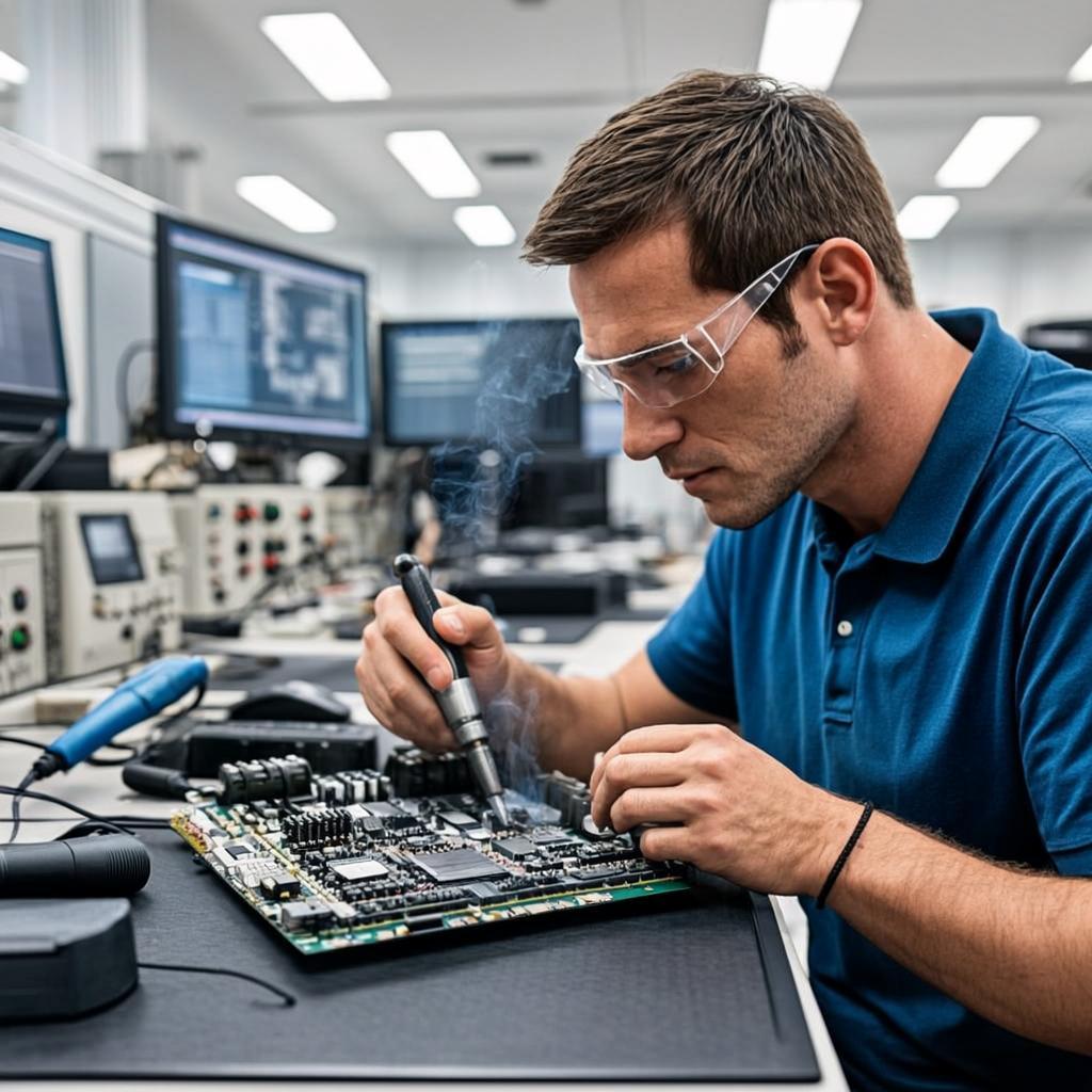
PTFE has “outstanding advantages,” but it is much more difficult to manufacture than ordinary FR-4. The core lies in solving 3 problems. In Teflon PCB manufacturing, the key manufacturing steps involved include specialized surface preparation, copper plating, drilling, and lamination, all of which require precise control and expertise. These complex processes are typically handled by experienced PCB fabricators who specialize in high-frequency and advanced material circuit boards.
The surface of PTFE is too smooth and inert, so copper foil easily peels off if directly attached. The current mainstream solution is “surface activation treatment”:
PTFE is relatively soft, so traditional mechanical drilling tends to cause burrs and deformation on the hole walls. Because of these challenges, manufacturers often favor ceramic filled laminates for their ease of drilling, improved structural integrity, and reliable via formation, especially in high-precision manufacturing processes.
Two methods are now used instead:
The solution is “stepwise heating + low pressure”:
Currently, PTFE PCBs mainly serve “high-end essential fields,” with 4 common application scenarios. When comparing various PCB materials, PTFE stands out due to its unique material properties, such as excellent dielectric performance and high heat resistance, making it ideal for advanced electronic and communication systems. The selection of PCB materials depends on the specific application requirements, with PTFE often chosen for its superior electrical and thermal characteristics. Commercial Teflon PCBs are widely used in industrial and commercial applications, including wireless communication devices and active safety systems, due to their cost-effectiveness and reliable high-frequency performance.