Choose FR - 4 copper - clad laminates with a high Tg (glass - transition temperature ≥ 180℃) and a low CTE (coefficient of thermal expansion ≤ 18ppm/℃), which meet the IPC - 4101 industrial - grade standard. This ensures that there is no base - material deformation in a wide - temperature environment. Use high - purity electrolytic copper for the copper foil (purity ≥ 99.9%). For power supply layers (such as inner layers carrying 24V/10A current), select 105μm - thick copper foil, and for signal layers, choose 35μm - thick copper foil to balance current - carrying capacity and wiring density.
Cut the base material to the designed size (with an error of ±0.1mm) using a CNC cutting machine. After cutting, perform "chamfering" on the board edges (45°, radius of 0.5mm) to prevent board - edge burrs from scratching operators or damaging equipment during subsequent processes. Also, reject base materials with edge corners missing or scratched to ensure a 100% initial base - material qualification rate.
The 16 - layer industrial control PCB board needs to fabricate 8 groups of independent inner - layer substrates first (such as layers 1 - 2, layers 3 - 4... layers 15 - 16), and then integrate them through lamination. The precision of inner - layer fabrication directly determines the signal integrity and power stability of the final circuit.
In a Class 10000 clean room, laminate a 35μm - thick photosensitive dry - film onto the base - material surface using a hot - pressing roller (temperature of 85℃, pressure of 0.6kg/cm², speed of 1.5m/min). During the lamination process, ensure uniform rolling to make sure the dry - film has no bubbles or wrinkles. If there are bubbles, subsequent exposure will cause incomplete circuits, affecting signal transmission.
Use Laser - direct Imaging (LDI) technology instead of traditional film exposure. The exposure accuracy reaches ±5μm, which is suitable for the fine - circuit requirements of the 16 - layer board (minimum line - width/line - spacing of 0.08mm/0.08mm). During exposure, use the optical positioning targets at the edge of the base material as a reference to ensure that the circuit position deviation of the same inner - layer substrate is ≤ 10μm, laying the foundation for subsequent multi - layer alignment.
Use an Automated Optical Inspection (AOI) device to fully inspect the etched inner - layer circuits, checking for open - circuits, short - circuits, line - width deviations, copper - slag residues, etc. Mark and rework non - conforming products to ensure an inner - layer circuit qualification rate of ≥ 99.8%. The high reliability requirements in industrial scenarios mean that inner - layer defects can directly cause the failure of the finished board.
To improve the bonding force between the inner - layer substrate and the inter - layer adhesive (prepreg PP), the etched inner - layer copper foil needs to undergo a "blackening → passivation" treatment:
Put the inner - layer substrate into an alkaline oxidation solution (mainly composed of sodium hydroxide and sodium sulfite) and react at 60℃ for 10min to form a black cuprous oxide layer (thickness of 0.5 - 1μm) on the copper - foil surface, increasing the surface area of the copper foil and enhancing the physical bonding force with PP.
After blackening, put the substrate into a chromate solution (concentration of 2%) and treat it at 40℃ for 5min to form a dense passivation film on the oxide layer surface, preventing the copper layer from oxidation and further enhancing the chemical bonding force with PP. After treatment, dry it (100℃, 15min) and test the inter - layer peel strength (should be ≥ 1.5N/mm) to ensure it meets the industrial - grade anti - vibration requirements.
Lamination is the core process in manufacturing the 16 - layer industrial control PCB board. It needs to solve three major problems: "multi - layer alignment accuracy", "inter - layer bonding stability", and "matching of material thermal expansion", ensuring that the laminated substrate has no warping, delamination, bubbles, etc.
According to the designed 16 - layer stacking scheme (such as the alternation of "signal layer - ground layer - power layer"), stack the inner - layer substrates and prepregs (PP, dielectric constant of 4.2, thickness of 0.1mm) in sequence on a clean workbench. The PP should cover the circuit area of the inner - layer substrate and extend 1mm beyond the edge of the substrate to ensure that the resin flows sufficiently during lamination to fill the inter - layer gaps.
Set 3 groups of optical positioning targets (diameter of 0.5mm, copper material) at the edge of each layer of the substrate. Automatically identify the targets through a CCD camera, adjust the position of each layer, and control the inter - layer alignment error within ±10μm. After alignment, fix the stacked structure with high - temperature - resistant tape to prevent misalignment during transfer.
Use a vacuum laminator for "step - by - step temperature - increasing and pressure - increasing". The specific parameters need to be adapted to the high - Tg base material and the multi - layer structure:
Put the stacked structure into the laminator, evacuate to ≤ 10Pa (removing the air between layers to prevent bubbles), then heat up to 120℃ (heating rate of 4℃/min), apply a pressure of 8kg/cm², and keep warm for 30min. At this stage, the PP starts to soften and initially fills the inter - layer gaps.
Continue to heat up to 180℃ (heating rate of 2℃/min), increase the pressure to 25kg/cm², and keep warm for 90min. The epoxy resin in the PP is completely cured, bonding the inner - layer substrates into one piece. The heating rate needs to be strictly controlled to avoid internal stress caused by the thermal - expansion differences of each layer of material, which could lead to substrate warping.
Stop heating, maintain vacuum and pressure, and naturally cool to room temperature (cooling rate ≤ 3℃/min). Take out the substrate after its temperature drops below 50℃. Rapid cooling will cause stress inside the base material, which may lead to inter - layer delamination, so the cooling curve must be strictly followed.
Visually check the surface of the laminated substrate for bubbles, delamination, indentations, etc. At the same time, use a laser thickness gauge to measure the substrate thickness (with an error of ±0.05mm) and a warpage tester to measure the warpage (should be ≤ 0.5%, meeting the installation requirements of industrial equipment).
Use an X - Ray device to observe the inter - layer alignment, ensuring that the inter - layer misalignment error is ≤ 25μm. Also, check the filling of the PP resin to ensure there are no voids or lack of glue, avoiding rough hole walls during subsequent drilling.
The outer - layer processing needs to complete "via metallization (realizing inter - layer interconnection) → circuit formation → surface treatment → shape processing" to ensure that the 16 - layer board has electrical connection functions and anti - environmental - interference capabilities.
The process is similar to that of the inner - layer, but it needs to adapt to the larger board area and more vias of the outer - layer. Form the outer - layer circuits (minimum line - width of 0.1mm) through LDI exposure (accuracy of ±5μm), development, and etching. After etching, conduct a full AOI inspection to ensure there are no open - circuits or short - circuits. Then print a temperature - resistant solder - mask ink (epoxy - resin material, thickness of 25μm) to cover the non - soldering areas, and bake at 150℃ for 60min for curing. Verify the reliability of the ink through a cross - cut test (adhesion ≥ 4B level). The solder - mask ink needs to have temperature - resistance and chemical - corrosion - resistance capabilities to adapt to the harsh industrial environment.
Process the substrate shape according to the design size through laser cutting (suitable for complex shapes, with an accuracy of ±0.05mm) or CNC punching (suitable for simple shapes, with higher efficiency). After processing, perform "deburring" on the board edges (burr height ≤ 0.02mm) to avoid scratching cables or operators during installation. At the same time, install metal bushings in the substrate fixing holes (such as screw holes) to enhance the mechanical strength and adapt to the vibration environment of industrial equipment (vibration test: 10 - 500Hz, acceleration of 5g, 1h for each axis without loosening).
The 16 - layer industrial control PCB board needs to pass triple inspections of "electrical performance + environmental reliability + mechanical performance" to ensure it meets the strict requirements of the industrial control field:
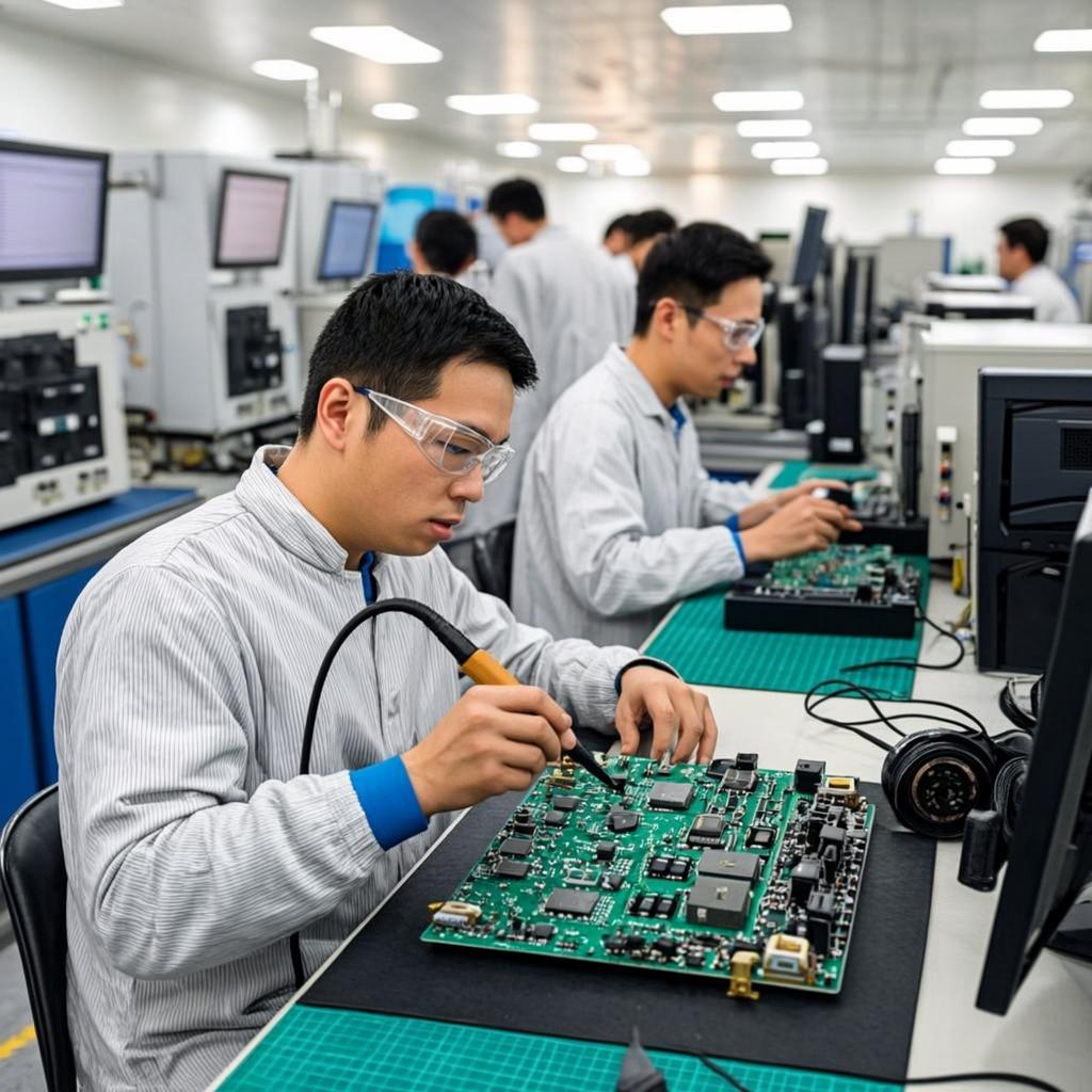
Use ICT in - circuit testing to check for open - circuits and short - circuits. Use a flying - probe tester to test impedance (such as the 50Ω impedance error of high - frequency signal layers ≤ ±10%), insulation resistance (≥ 10¹⁰Ω), and conduct a withstand - voltage test (500V AC, 1min without breakdown) to avoid the risk of electric leakage.
Conduct a thermal shock test (-40℃/30min → 85℃/30min, 100 cycles without delamination), a damp - heat test (85℃/85% RH, 500h without oxidation), and a salt - spray test (5% sodium chloride solution, 48h without corrosion) to verify the stability of the substrate in harsh environments.
Conduct a bending test (bending radius of 10mm, 100 times without breakage) and a peel - strength test (inter - layer bonding force ≥ 1.2N/mm) to ensure that the substrate has anti - vibration and anti - impact capabilities.