Helen Frankenthaler PCB Circuit Board R&D Center

alumina ceramic pcb kit

Ceramic PCB

Ceramic PCB Material Available

  • Alumina (Al2O3) - The mechanical strength, chemical stability, thermal conductivity, and electrical properties of Al2O3 are advantageous compared to other oxide ceramics. The abundance of raw material makes alumina the most commonly used ceramic substrate material. Al2O3 ceramic PCBs are used in automobile sensor circuits, shock absorbers, and engines. The high thermal stability of Al2O3 ceramic PCBs improves the performance and thermal efficiency of the circuits used in automobiles.

  • Aluminum Nitride (AlN) - The high thermal conductivity and coefficient of expansion are two properties that make AlN noteworthy as a substrate material in the PCB industry. The thermal conductivity of AlN varies in the range of 170 W/mK to 220W/mK. The CTE of AlN ceramic matches with silicon semiconductor chips, which establishes a good bonding between the two, thus making their assembly reliable. AIN is used in sensor circuits in automobiles, as it can withstand extreme temperatures, corrosion, and vibration while providing efficient, accurate, and sensitive sensor signals.

  • Beryllium Oxide (BeO) - BeO is a ceramic PCB substrate material with a thermal conductivity around nine times that of Al2O3 and greater than metal aluminum. BeO showcases better chemical stability than AlN and high electrical isolation comparable with Al2O3e. BeO is used in applications where the PCB is subjected to high temperatures or in high-density PCBs facing space limitations to provide air or liquid cooling.

Aluminum oxide PCB (Al2O3 or Alumina) solutions

Aluminum oxide PCB (Al2O3 or Alumina) is today the most widely used ceramic printed circuit board and submounts. This is thanks to its good material properties, namely good thermal conductivity, low CTE (coefficient of thermal expansion), resistance to chemical hazards and hermeticity in combination with a relatively low cost and a more easy handling. Applications include for example cooling and heating modules, LED boards, medical circuits, sensor modules, and high-frequency devices.

The main reasons Alumina is chosen over other printed circuit boards is:

  • Higher operating temperature up to 350ºC (using thick film printing)
  • Lower expansion coefficient (6-8 ppm/ºC) matching components
  • Good thermal properties (22-24 W/mK)
  • Superior high-frequency performance
  • Smaller package size due to integration and multi-layer possibilities
  • High wear and chemical hazards resistance
  • Hermetic packages possible, 0% water absorption
  • Good light reflection due to white color.
  • Limited to no outgassing
  • Strong rigid material

At Hemeixin, we supply both Aluminum Oxide PCB (Al2O3 96%) made by thick film process (Silver metalization) as well as Direct Plated Copper Technologies (DPC), with copper tracks and pads.

Aluminum Nitride PCB solutions

Aluminum Nitride PCB (AlN) is one of the best performing circuits solutions today for high current or high temperature electronics. Thanks to its incredible thermal conductivity (170 W/mK) and dielectric strength combined with its low thermal expansion (CTE <4 ppm/C) it is used today in many application ranging from high power LEDs and lasers to high current switches, ultra low temperature vacuum chamber electronics (e.g. quantum computing) and many many more … . Furthermore it has all the additional benefits other ceramic material have like rigidity, resistance against environments & chemical hazards and 0% water absorption.

The main reasons Aluminum Nitride is chosen over other printed circuit boards is:

  • Superior thermal conductivity 170W/mK
  • Strong dielectric
  • High operating temperature >350ºC possible
  • Low expansion coefficient <4 ppm/C
  • Smaller package size due to integration
  • Hermetic packages possible, 0% water absorption
  • Limited to no outgassing

At Hemeixin, we supply both Aluminium Nitride PCB (AlN) processed by thick film process (Silver/silver palladium metalization) as well as Direct Plated Copper Technologies (DPC), with copper tracks and pads.

Ceramic PCB Design Guidelines

1.Ceramic PCB Material

Item Spec
Standard material AL2O3(92%,95%,96%)
AIN(thermal conductivity 170-200W)
Material need special control AL2O3(99%)
AIN(thermal conductivity 200-230W)
Material need evaluation Zirconia,Beryllium oxide,silicon nitride,quartz glass

2. Ceramic PCB Material specification

Item Spec
Common material size 50mmX50mm 120mmX120mm 140mmX190mm
Special material size Materials out of spec of above mentioned size need evaluation.

3. Ceramic PCB Material thickness

Substrate typeSubstrate thickness(mm)
AL2O3\AIN ceramic pcb0.38, 0.5, 0.635, 0.8, 1.0,1.2,1.5, 1.8, 2.0,2.5, 3.0
Material need special control AL2O30.125,0.2,0.25,0.3
AIN0.25,0.3
Material need evaluationMaterials out of spec of above mentioned size need evaluation.

4. Ceramic PCB Laser drill

Board thickness(mm)Standard(um)In advance min hole size(um)
0.258060
0.38060
0.3810080
0.5120100
0.635180150
0.8200180
1.0250200
1.2300250
1.5380300
2.0500300

When board thickness >2.5mm, board thickness/hole size ≧4:1,or min hole size out of above spec,evaluation is needed. Hole to hole space:0.25mm or larger.

5. Line with/Line space

Copper thicknessStandard
18(um)60(um)
30(um)≥75(um)
60(um)≥100(um)
80(um)120(um)

Evaluation is needed when line width/space smaller than 50um, or line width/space smaller than above data.

6. Solder mask and silkscreen

ItemStandardIn advanceNeed evaluation
Solder mask colorGreen, blue, yellow, red, light green, matte green, matte blue, matte black transparent, gray,Neon greenOther colors
Solder mask damGreen: 120um Other colors:150umGreen:100um Other colors:120umSmaller width than left columns.
Silkscreen colorBlack, whiteSame as standard solder mask colors.
Silkscreen height≥800(um)≥650(um)Smaller height than left columns.

7. Surface finish and thickness

Standard surface finish and plating thicknessSpecial controlled surface finish and plating thickness
Hard gold plating(um) NI:3.05-5.08, AU:0.127-2 ENEPIG(um) NI:3.05-5.08, PD:0.025-0.2, AU:0.025-0.2 Immersion silver: 0.2-1 Immersion Tin: OSP: 0.2-0.6 HASL (LF)ENIG:(um) NI:5.08-6.35, AU:0.2-0.76Hard gold plating(um) NI:5.08-6.35, AU:2-4 ENEPIG(um) NI:5.08-6.35, PD:0.2-0.5, AU:0.2-0.76

Evaluation is needed when hard gold plating area bigger than 50%, silver plating and other plating thickness exceed above parameters.

8. Outline process

ProcessToleranceMax board size
Laser cutting±0.1mm130*140mm
Water Jet Cutting±0.1mm130*140mm

Evaluation is needed when tolerance exceed above parameters.

ItemRequirement
Laser pre cutting(lineation)Standard technique, board thickness 0.5mm, pre-cut depth15-30%. Special controlled, board thickness 0.38mm, pre-cut depth 10-15%. Evaluatoin is needed when board thickness less than 0.38mm, and laser pre cutting is required.
ItemRequirement
Laser cuttingStandard technique: board to board space ≥0.25mm Special controlled: board to board space ≥0.2mm
Water Jet CuttingDepends on blade width
Othersneed evaluation.

Ceramic PCB Capabilities

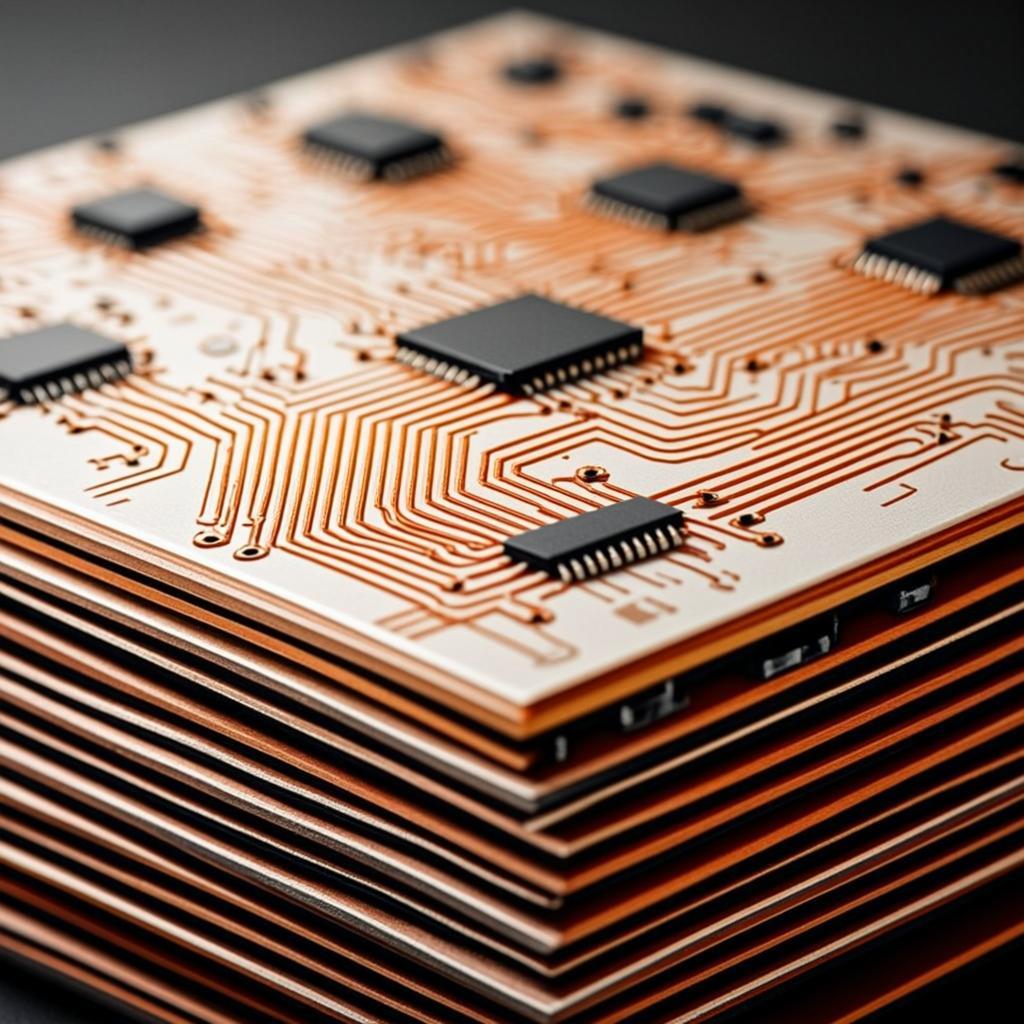
Compared with regular substrates like glass epoxy (FR4) or aluminium (Al), the ceramic substrate is an ultra-thin composite structure. It offers superb electrical insulation, high thermal conductivity, high adhesion strength. Because of these characteristics, a ceramic substrate PCB has higher current carrying capacity, while it is possible to etch it just like a regular board can. With harsh weather resistance capabilities, ceramic PCBs are suitable for harsh outdoor environments. Ceramic PCBs are eminently suitable for product that generate high heat, such as solar energy equipment and high-brightness LEDs do.Alumina PCB and Aluminum Nitride PCB solutions below:

Direct plated copper (DPC)Technology

Process ItemMP capability
Standard Layers1-2L
Base material thickness0.15-2.5mm
Board thickness tolerance±10%
Warpage≤0.7%
Laser drill Min laser hole size0.06mm
Hole tolerance PTH±0.075mm
NPTH±0.025mm
Electroplating aspect ratioThrough hole 4:1
Electroplating filling via Filling via size0.07-0.25mm
Layout design Max base copper Outer layer≤100um
Line width/space (outer layer)Copper thickness 10-35um3/3mil
Copper thickness 35-100um4/4mil
Line width tolerance Line width≥10mil±2mil
Line width<10mil±20%
Pad size tolerance Pad size≥12mil≥±10%
Box dam height150um-1200um±50um
Outline Laser cutting or water jet cutting Outline tolerance≤±100um
Max board size130*180mm
Surface finish Hard gold plating Gold thickness0.127-2um
Nickel thickness3.05-5.08um
ENIG Gold thickness0.025-0.76um
Nickel thickness3.05-5.08um
ENEPIG Gold thickness0.025-0.76um
Palladium thickness0.025-0.2um
Nickel thickness3.05-5.08um
OSP Film thickness0.2-0.6um
Immersion silver Silver thickness0.2-1um

Direct Bonded Copper and Active Metal Brazing Technology

Process ItemMP capability
Standard Layers1-2L
Base material thickness0.38-1.0mm
Board thickness tolerance±10%
Warpage≤0.7%
Laser drill Min laser hole size0.15mm
Hole tolerance PTH/ NPTH±0.1mm
Aspect ratioThrough hole 4:1
Layout design Max base copper thickness Outer layer127-400um
Copper thickness 0.127mmSpace: 0.30mm
0.20mmSpace: 0.35mm
0.25mmSpace: 0.40mm
0.30mmSpace: 0.45mm
0.40mmSpace: 0.55mm
Line width tolerance Line width≥10mil±2mil
Line width<10mil±20%
Pad size tolerance Pad size≥15mil≥±10%
Outline