This guide has everything you’re looking for about ultra-thin PCB such as classification, quality standards, co-efficient of thermal expansion, and applications, amongst others.
So, if you want to be an expert in ultra-thin PCBs, read this guide.
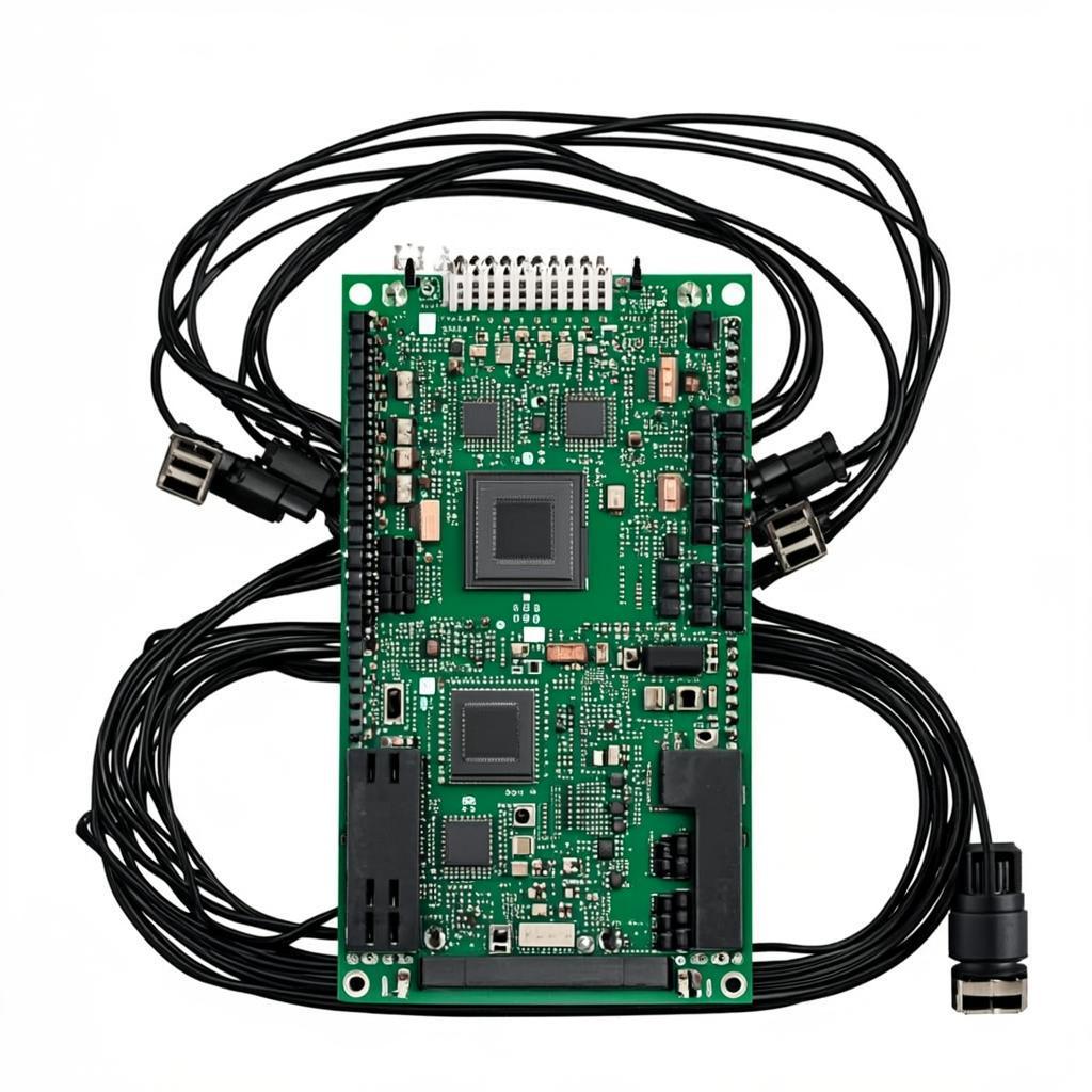
As the name suggests, extra thin PCB is a type of printed circuit board with a smaller thickness than standard PCB.
It is lighter and more compact since it has decreased board materials and volume of copper features.
Ultra-Thin PCB is ideal for PCB applications where miniaturization and high level of reliability serve a key role.
It facilitates miniaturization with enhanced performance through higher-density PCB designs.
Ultra thin PCB
The following are the main benefits of Extra-Thin PCB:
All lines of ultra-thin PCB are configured, which saves time during connection of excess lines.
This type of PCB can effectively minimize the final product volume, making it conveniently portable.
Thinner PCB materials result in smaller vias, less copper plating, smaller spaces and lines and decreased aspect ratio of vias. This leads to a more compact and lightweight PCB product.
Miniaturization in the X- and Y-axis can considerably minimize the footprint of ultra-thin PCBs. However, Z direction miniaturization allows more space for supplementary components and minimize the general thickness of the circuit board.
Other benefits of ultra-thin PCB include easy assembly, good solderability, low general cost and good heat dissipation, among other factors.
The design of extra thin PCB as well compensate for the inadequacy of the PCB substrate in relations to component carrying capacity.
There are three main types of extra thin PCB including:
There are ultra-thin rigid PCB materials for applications requiring a 2D printed circuit board.
They are usually applied as packaging substrates for integrated circuits, in which they aid in making the whole component extremely thin.
You can attain 25 microns wide spaces or lines, pitches below 175 microns, and 50 and 100 microns vias and pads diameters respectively.
Also referred to as flex ultra-thin PCB, this is a type of extra-thin PCB manufactured using flexible laminates.
This allows folding of the PCB, which reduces the volume and surface area required to house the board, hence increasing the integration density.
Moreover, PCB equally facilitates better bending.
This implies that it is practical bend the circuit board through smaller bend radii, making it possible to attain even tinnier volumes.
One of the main applications of ultra-thin flexible PCB due to their advanced bending capability is manufacture of cables requiring dynamic bending.
These types of extra thin PCB feature conductors on the rigid and flexible layers of the printed circuit board.
Plated thru-holes stretch between the rigid and flexible segments and electrically link multiple layers of conductor.
Through integration of rigid sections to the flexible components, it allows you to enhance the design abilities of your ultra-thin PCB.
The rigid segments offer perfect hard mounting locations for components, chassis and connectors.
On the other hand, the flex segments provide dynamic flexing, flex-to-fit and vibration-resistance zones.
Such combination gives you multiple choices for achieving innovative solutions for the greatest demanding rigid flex PCB applications.
Here are the some of the uses of ultra-thin PCB:
High-Density Interconnect PCB is simply an ultra-thin PCB having more counts of interconnections, covering minimal space, leading to circuit board miniaturization.
The components of HDI PCB are positioned closer, reducing the board space significantly but not compromising its performance.
HDI PCB
HDI is among the fastest advancing PCB technologies, capable of integrating smaller capture pads and vias and higher densities of connection pad.
HDI PCBs have buried and blind vias and usually comprise of microvias with diameter of 0.006 or lower.
Extra thin HDI PCBs provide better construction, layout and design choices by integrating outstanding features like microvias.
They give smaller form factor, increased functionality, and highly dense ultra-thin flex circuitry.
Moreover, though they employ thinner PCB materials, HDI boards offer improved electrical performance, better reliability and advanced extra thin PCB.
By applying HDI technology, it is possible to mount more components on either surfaces of the Ultra-thin PCB if necessary.
Additionally, with the advancement of blind via and via in pad technology, you can position smaller components nearer to each other.
This signifies quicker signal transmission and substantial reduction in crossing delays and signal loss.
The common applications of Ultra-thin HDI PCB include use in:
There are three different techniques of drilling microvias in ultra-thin PCB:
This method of microvia drilling etches PCB material for formation of hole using plasma.
With this technique, you can attain a via hole diameter of 75 µm via hole diameter on a 25 µm thick material.
However, coupled with costs on special vacuum machinery, plasma etching makes the least promising technique for via hole drilling.
Photo-via technology employs lithography patterning and photo-imaginable dielectric material.
The method has promoted the advancement of ultra-thin HDI PCB.
It features a hole size of approximately 25 µm for both depth and diameter.
However, it is an expensive method of drilling ultra-thin PCB microvias because of the unique dielectric material.
This is the most promising microvia drilling technology.
Through laser drilling, you can attain via hole diameter as low as 5 µm on a dielectric material with 5 µm thickness.
The main factors controlling this technique of microvia drilling is energy density, substrate material, wavelength, and thickness of substrate material.
It is the most preferred drilling method for microvias, which involves focusing a laser beam on an extremely small area.
The vias created incline to be as clean as those developed through mechanical drilling.
This ensure uniform deposition of plating on the vias interior.
Laser via drilling features a reduced drill speed in comparison to mechanical drilling.
The technique can be applied to effortlessly bore dense microvias in an Ultra-thin PCB, applying wavelengths spanning from ultraviolet to deep infrared.
However, the main disadvantage of laser via drilling is the limited laser beam depth that you can reliably and reproducibly drill.
When one lens is utilized for beam concentration, the depth drillable by the laser is limited because of the restricted depth of focus.
But, a collimated laser beam enables laser via drilling to a deeper depth.
Nevertheless, the challenge with it is the extremely small via size, which causes Fresnel diffraction in the beam.
This can in turn impact on the beam intensity in exceptionally deep microvia holes.
Types of vias
Polyimides prepregs are more sensitive to moisture than epoxies by the fact that they tend to absorb moisture from air faster.
Moisture within the prepreg does it little harm, though may lead to delamination, voids and other flaws in laminated ultra-thin PCBs.
A perfect indicator of moisture in PCB prepreg is foamy flow, which is common with polyimide because they absorb moisture faster.
Vacuum drying or storing any prepreg with desiccant at low humidity will reduce this effect.
Moisture can result in additional issues in finished ultra-thin PCB.
Excessive moisture can compromise the integrity of a multiple layer PCB under high temperature strained environments.
Therefore, it is crucial to regulate moisture even in complete bare circuit boards before solder reflow or PCB assembly process.
Moreover, controlling moisture is equally essential in finished ultra-thin PCB in case they will be eventually subjected to high temperatures.
It is advisable to vacuum dry prepregs at 29 of vacuum for several hours.
Vacuum desiccation under room temperature is the most preferred over any form of oven drying for ordinary polyimide or epoxy PCB prepreg.
It is the best method of drying ultra-thin PCB prepreg even if the oven drying process is subjected to controlled conditions.
Oven drying may incline to enhance the prepreg, and might lead to marginal or inadequate bonds or flow.
This can cause delamination or additional failures on succeeding thermal processing.
Nonetheless, Non-woven aramid polyimide is the only exception.
Here, oven temperature not exceeding 32 degrees Celsius at 29 of Hg for 4 – 5 hours may help in eliminating excess moisture.
Some of the important quality standards for Ultra-thin PCB include:
Ultra think PCB
The main goal in ultra-thin PCB fabrication is to have more trace routing to smaller sections as PCB density increase with technology.
This has resulted in use of embedding vias as well as buried and blind vias in surface mounted pads.
Nevertheless, buried and blind vias are more challenging to fabricate due to the additional drilling procedures involved.
Moreover, the drilling may leave debris in the holes leading to manufacturing flaws.
Ordinary vias are equally often too broad to be integrated in the tiny surface mount pads found in modern high density PCBs.
However, microvia can assist with all these challenges:
Here are some of the key shortcomings of ultra-thin PCB:
Ultra-thin printed circuit boards are designed and constructed for distinct applications.
This leads to high initial cost of PCB design, layout and photographic plating.
Therefore, it is advisable not to use them in small amounts.
Once fabricated, extra thin PCB must be modified from the configured lithography program or base map, making it hard to change.
Moreover, it has a protective layer on the surface, which should be removed prior to repairs. Removing and restoring the surface covering is a fairly challenging task.