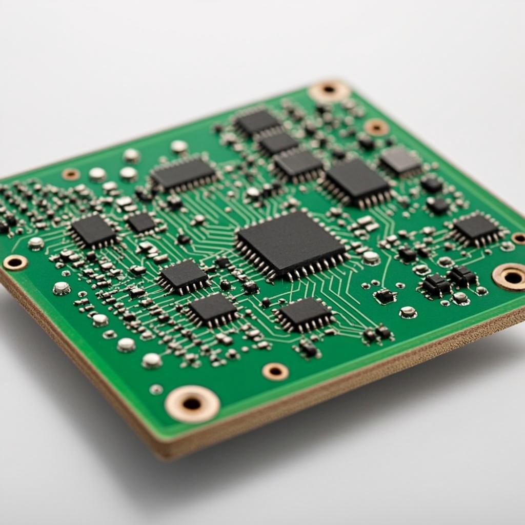
The Printed Circuit Board (PCB) serves as the foundation of an electronic circuit, the bare board produced through fabrication processes like etching, drilling, and applying protective layers. The PCB itself carries no active function. The Printed Circuit Board Assembly (PCBA) is the realized circuit function, where all electronic components (resistors, ICs, connectors) have been mounted and soldered onto the PCB. The PCBA stage involves automated PCBA component placement, soldering (reflow or wave soldering), and quality testing. Understanding this sequence is crucial: PCBA reliability is constrained by decisions made during the bare PCB design.
Industry consistency, reliability, and manufacturability depend on adherence to standards published by the IPC (Association Connecting Electronics Industries). These standards are widely adopted in industry practice and are often specified by OEM/EMS contracts and quality systems as acceptance criteria or design basis.
This standard is fundamental to Design for Manufacturability (DFM). It dictates the specific land pattern dimensions (footprints) for Surface Mount Devices (SMD) to optimize their behavior during automated assembly processes. Compliance ensures compatibility with standard manufacturing processes and guarantees reliable solder joints with proper toe, heel, and side fillets, actively preventing defects like tombstoning or solder bridging during reflow. This standardized geometry ensures predictable wetting and placement accuracy in high-precision pick-and-place and reflow systems. This predictability directly increases First Pass Yield, thereby minimizing rework, scrap, and operational costs. Thus, the economic function of IPC-7351 lies not only in reliability but also in promoting manufacturing predictability through standardization.
This document defines the ultimate quality benchmark. It outlines the acceptance criteria against which quality assurance and inspection are performed, categorized by the product's intended reliability class. Compliance dictates the acceptable quality of solder joints, component placement, and rework standards.
The vast majority of components on a PCBA are passive Surface Mount Devices (SMDs), such as chip resistors and capacitors. Their small sizes make them highly susceptible to assembly defects.
Tombstoning (where the component stands on one end) is a common failure mode that predominantly affects small two-terminal passive components (like 0402, 0603 packages).
Tombstoning occurs during reflow soldering: as the molten solder on one pad wets the component lead and exerts a pulling force, the resulting asymmetrical surface tension can lift the low-mass component vertically if the solder on the opposing pad has not yet melted and wetted. This demands strict control over the symmetry of heat application.
Diodes, LEDs, and TVS diodes are polarized components that allow current flow in only one direction (anode to cathode). Incorrect orientation will render the circuit non-functional.
To support both manual assembly and Automated Optical Inspection (AOI), clear and unambiguous polarity markings must be provided on the silkscreen layer.
The recommended practice is to mark the cathode (negative terminal). Clear options include the schematic diode symbol, a simple straight line marking the cathode end, or the letter 'K' (to denote cathode, avoiding confusion with the 'C' for capacitors).
Using only the '+' or '-' symbols can be ambiguous and is therefore not recommended: For some devices (e.g., TVS diodes), the circuit potential may not align intuitively with the component's internal polarity (e.g., cathode connected to a positive rail). This ambiguity increases the risk of misplacement by assembly operators and can confuse automated inspection systems.
Complex packages characterized by hidden solder joints and high thermal requirements necessitate specialized design and assembly solutions.
QFN packages utilize exposed thermal pads, requiring precise solder paste control to manage heat and prevent defects.
The large exposed pad beneath the QFN is crucial for thermal management, relying on an array of thermal vias to conduct heat vertically to internal ground or power planes.
Voids (air pockets) in the thermal pad solder joint severely degrade thermal conductivity, leading to localized overheating.
To control solder volume and reduce the risk of voids and surrounding pin bridging, the stencil aperture for the thermal pad must be reduced. DFM standards typically require reducing the printed solder paste area by 20% to 50% to ensure an appropriate volume of paste deposition.
BGAs are critical high-density ICs that rely on solder balls for connection. Their fine pitch necessitates the use of Via-in-Pad (V-I-P) technology for efficient routing.
V-I-P places a plated hole (via) directly inside the component's solder pad. This technique is essential for routing fine-pitch BGA breakouts (HDI boards). V-I-P Manufacturing Complexity: Fill and Planarization V-I-P introduces significant cost and process complexity because the vias must be filled and planarized (capped and plated over).
V-I-P is justifiable in compact, high-performance applications (e.g., smartphones, high-speed servers) where the space saved, improved signal integrity, and superior thermal performance outweigh the significantly increased cost. While V-I-P increases upfront Non-Recurring Engineering (NRE) costs and process steps, the competitive advantage gained from m