These boards are generally used in consumer devices like microwave ovens and high-bandwidth communication systems that operate at a very high frequency range (1 GHz to 30 GHz).
In this blog, you will learn the critical aspects of microwave PCB design, including material choices and the application of coplanar waveguides (CPW).
When designing microwave PCBs:
When choosing a dielectric material for microwave boards, consider the following crucial properties of the dielectric material.
The dielectric constant measures a material’s ability to store electrical energy in an electric field.
D k impacts the high-frequency operation, making it a primary concern for RF and microwave circuit boards. Therefore, select materials based on their performance in different frequency conditions.
The dielectric constant influences the speed at which electromagnetic signals propagate through the PCB substrate. D k directly impacts signal delay and phase shift.
For microwave PCBs, choose materials with a relatively constant D k across a wide range of frequencies. The lower the D k value, the better, typically in the range of 2 to 4 at 10 GHz.
The dissipation factor (D f) is a vital parameter that indicates a material’s efficiency in converting electrical energy into heat. For microwave PCBs, lower D f values are preferred to minimize signal losses and ensure reliable performance.
For instance, RO3003 exhibits a D k of 3 and a D f of 0.0013, whereas RO4350B has a D k of 3.66 and a D f of 0.0031, making RO3003 the preferable choice due to its lower signal loss.
Choose a lower D f (<0.005) material for radio-frequency and microwave applications.
The coefficient of thermal expansion (CTE) measures the rate at which a material expands or contracts with temperature changes. In multilayer PCBs, CTE mismatch between layers can cause mechanical stress, warping, and potential reliability concerns.
Ideally, the CTE values of all materials used in a circuit board stack-up should be similar and closely match copper’s CTE. Significant differences in CTEs can cause thermal stress on the board at high frequencies.
For microwave boards, choose materials with low thermal expansion coefficients of 10 to 20 ppm/°C in the z-axis to maintain dimensional stability under varying temperatures.
The choice of substrate thickness depends on operating frequency, dielectric constant, and application requirements. It is typically in the range of 10 to 125 mil. The optimal substrate thickness can be chosen based on the specific design goals.
Always pick thinner substrates (10 to 20 mil) for frequencies above 10 GHz to avoid signal integrity issues.
Loss tangent (tan δ) is the signal loss caused by energy dissipation within the PCB substrate.
This dimensionless parameter is determined by the phase angle between the resistive and reactive components of a system. For instance, a capacitor should ideally exhibit only capacitance (C). However, real-world scenarios such as equivalent series resistance (ESR) contribute to the loss tangent.
Evaluating loss tangents is crucial in the material selection process for high-frequency applications. Materials with low loss tangents effectively minimize signal attenuation and distortion.
Typical values for loss tangent range from 0.0022 to 0.0095 within the 10-30 GHz frequency range.
Moisture absorption is a critical factor in microwave PCB materials, as moisture can significantly impact the dielectric properties and overall circuit performance.
In indoor settings, moisture absorption may not be a primary concern. However, in environments with high humidity, this characteristic becomes extremely important.
Water molecules have a high dielectric constant and can increase the dissipation factor of the laminate, leading to increased signal loss and degraded performance.
Microwave PCB materials are designed to have low moisture absorption rates to maintain stable dielectric properties and minimize the impact of environmental factors. Laminates with moisture absorption rates below 0.1% are suitable for microwave applications.
Materials such as PTFE and ceramic exhibit excellent moisture resistance. They are inherently hydrophobic and have minimal water absorption, making them ideal for applications exposed to humid environments.
Materials that meet all the above requirements include ceramic, fiberglass, and PTFE (Teflon). Among these, PTFE has the lowest dielectric constant (typically 2.6~2.7) and loss tangent (0.002). PTFE is the most widely used material for manufacturing microwave PCBs.
However, metallization is challenging for PTFE as the surface is smooth. To overcome this, at Sierra Circuits, we perform plasma and sodium etch (for thicker boards) treatments before plating to improve laminate metalization.
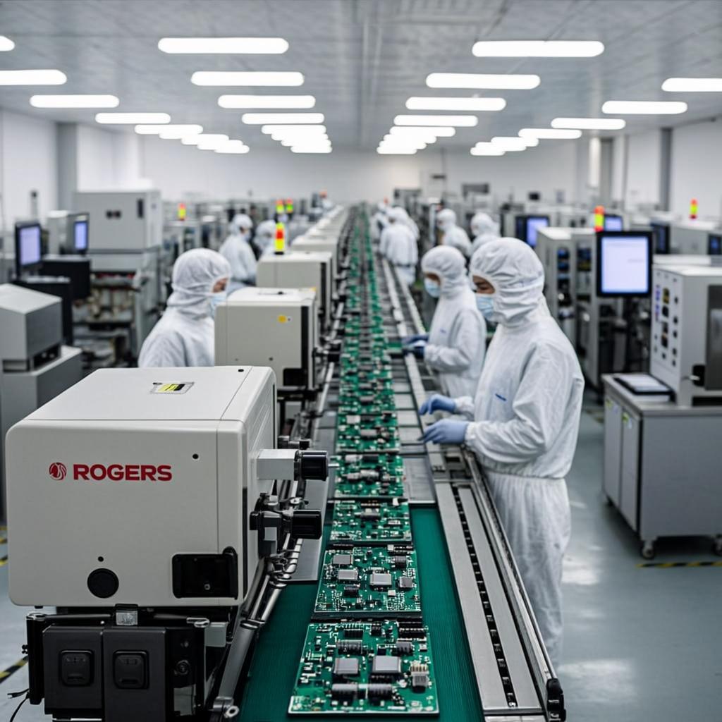
Sierra Circuits fabricates high-quality RF and microwave boards with operating frequencies ranging from 10 MHz to 30 GHz.
PTFE, polyimide, and cyanate ester (D k = 2.5) are good substrate choices for microwave PCBs. Below are a few examples of such dielectric materials:
When assembling microwave PCBs, select bonding materials such as fluorinated ethylene propylene (FEP), ceramic-filled PTFE, and liquid crystal polymer (LCP). These materials offer low lamination and re-melt temperatures to maintain optimal performance.
Opt for hybrid multi-layer circuit boards for critical, performance-driven applications. By combining different materials for various layers, such as using Rogers material for RF layers and FR4 for standard component layers, you can achieve the desired properties while optimizing costs.
This approach broadens the range of dielectric constants and thermal tolerances, ensuring efficient performance without compromising on budget constraints.
In addition to dielectric materials, the transmission line geometry is important in maintaining signal integrity in a microwave PCB.
Coplanar waveguides operate in a quasi-TEM mode, where a negligible portion of the EM field extends outward. This provides low dispersion and minimal dielectric loss, maintaining strong signal quality across a broad frequency range.
As an RF engineer, you should know about the coplanar waveguide structure, as it is the preferred trace geometry to route microwave signals with signal integrity.
In our recent webinar, resolving common errors in RF PCB layout design, we surveyed 30 PCB designers, out of which 46.7% shared that they occasionally use coplanar waveguides in their microwave boards, while 33.3% have never incorporated them.
In the next section, we will explain the benefits of incorporating CPWs in your designs.
Various PCB transmission line options, such as microstrip, stripline, and CPW, are available, but their selection depends on factors like:
On the higher end of the frequency spectrum, a coplanar waveguide is recommended.
CPWs are becoming more prominent in microwave PCB designs, especially for high-frequency applications, because it is compatible with millimeter-wave technology.
CPWs are primarily utilized for creating printed antennas, as they offer advantages over standard microstrips and discrete component-built antennas.
The central conductor serves as the feed for the antenna, where the input signal is applied. The ground planes provide a return path, which is crucial for maintaining signal integrity.
The signal line in CPWs terminates in a square or rectangular patch, enabling the antenna to direct signals perpendicular to the board surface.
In contrast, traditional microstrip antennas often exhibit higher levels of cross-polarized radiation, resulting in reduced power output efficiency and increased thermal dissipation, which can accelerate board aging.
Design and performance: