"A multilayer PCB has more than two copper layers. Multilayer PCBs save space and increase circuit density. PCB layers are possible up to 64 at the multilayer PCB manufacturer PCBONLINE."
MATERIALS For FR4 multilayer PCB, PCBONLINE uses high-Tg Material by default, and multilayer flexible, rigid-flex, aluminum, copper, and ceramic PCBs are available.
EQUIPMENT At PCBONLINE, there are special-purpose production lines for immersion gold, which are lacking at most multilayer PCB manufacturers in the world.
TEAM The professionals from PCBONLINE can optimize multialer PCB design and provide professional one-on-one engineering support throughout your project.
QUALITY PCBONLINE has set up an ISO quality management system, and its multilayer PCB is certified with ISO 9001, IATF 16949, RoHS, REACH, UL, and IPC.
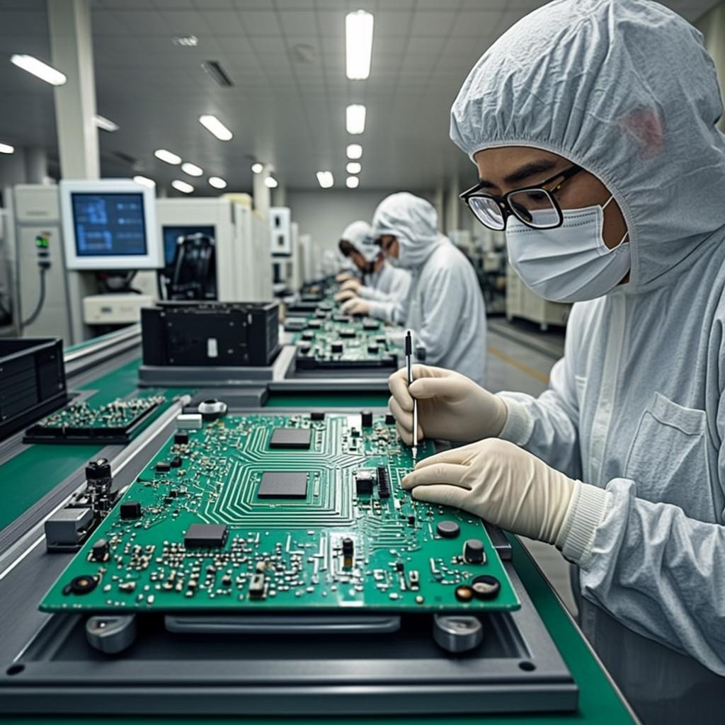
CUSTOM PCBONLINE provides multilayer PCB fabrication and assembly on demand, including design for manufacturing (DFM), PCB design, prototype, assembly, testing, and delivery.
TRANSPORT PCBONLINE provides various multilayer PCB shipping methods, including air, sea, and rail shipping by DHL, FedEx, and UPS. You can choose your freight forwarder.
Multilayer PCBs are printed circuit boards with 3 copper layers and above.
The core materials of multilayer PCBs can be FR4, aluminum, copper, PI, PET, PTFE, ceramics, etc. Components can mount on one side or both sides.
There are multilayer FR4 PCB, multilayer flexible PCB, and multilayer ceramic PCB. And rigid-flex PCB, HDI PCB, rigid-flex PCB, and high-frequency PCB belong to multilayer PCB.
To reduce the warpage, multilayer PCBs usually have a symmetrical structure. Typically, multilayer PCB has 4, 6, 8, 10, 12, or 16 copper layers.
At PCBONLINE, the wiring on multilayer PCBs is possible on up to 60 and 64 layers.
Multilayer PCB feature: higher wiring density smaller product sizes more circuit design flexibility Via the ground and power layers, multilayer PCBs reduce EMI (electromagnetic interference)
The multilayer PCB manufacturing workflow is: Cutting laminate > generating circuit in inner layers > lamination > drilling > copper plating > generating circuit in inner layers > automatic optical inspection (AOI) > solder mask and silkscreen > surface finish > profile > electrical test > final quality control > packaging.
In multilayer PCB fabrication, the lamination process must have no air trapped in the board, the resin in the prepreg melts and cures and the two adjacent conductive layers are bonded and insulated.
Before generating circuits in the outer layers, on the inner layers, there should be an oxidation layer, which roughens the copper surface to integrate with prepreg.
If the oxidation is Cu₂O, we call the multilayer PCB manufacturing method the "brown oxid" process; if the oxidation is CuO, we call the method the "black oxide" process.
At the one-stop multilayer PCB manufacturer PCBONLINE, you can have any kind of multilayer PCB manufactured and assembled. The PCB layer quantity to fabricate is below: FR4 multilayer PCB: 4-layer PCB, 6-layer PCB, 8-layer PCB, 10-layer PCB, 12-layer PCB, 16-layer PCB... 60-layer PCB, and 64-layer PCB Ceramic multilayer PCB: 4-layer PCB Rigid-flex PCB: 3-layer PCB, 4-layer PCB, 6-layer PCB, 8-layer PCB, 10-layer PCB, 12-layer PCB... 24-layer PCB Flexible multilayer PCB: 4-layer PCB, 6-layer PCB, 8-layer PCB High-frequency PCB: 4-layer PCB, 6-layer PCB, 8-layer PCB, 10-layer PCB... 24-layer PCB
If you need multilayer PCB prototypes and bulk production, you can send your Gerber to pcb@frankenthalerfoundation.org to get a quote or chat online with PCBONLINE.
Applications of multilayer PCB: computing, telecommunication, medical devices industrial controls, automotive equipment defense & aerospace systems consumer electronics, etc.
File Upload Select file Please upload the file in only the zip, rar, or 7z formats. Submit
ISO IPC IATF RoHS REACH UL
"PCBONLINE once manufactured 12-layer PCBs for a client. The PCB requires very high FPGA manufacturing precision and PAD tolerance control in engineering and fabrication. Under the microscope, the circular PADs are not deformed at all, and the integrity of the solder mask bridge is well protected."
"PCBONLINE manufactured and assembled this complex multilayer PCB. In the DFM stage, our engineer found a design issue and helped our customer avoid possible economic losses. According to our customer, our assembly price is at least 40% less than assembly in Europe."
"This is a 12-layer PCB used for engine turning. PCBONLINE manufactured it for a U.S. customer. At first, our customer designed the copper thickness of the traces to be 6oz. But the effect was not very good. So our engineer made testing and advised 4oz copper thickness. The product finally yielded excellent results."
PCBONLINE has rich experience in multilayer PCB design, fabrication, and assembly. Read our blogs to explore more details of multilayer PCBs. take a look
4 Layer PCB manufacturing [7 Steps with Images]
6 Layer PCB Manufacturing - How is 6-layer Circuit Board Made
1 Learn about our products 2 Support Request 3 Get customized services
Offer Electronics Manufacturing All-in-One PCBONLINE® is a registered trademark or service mark of pcb online limited or its affiliates. Copyright © 2005-2025 Pcb Online Limited. All rights reserved
Star Products PCB Assembly Box-Build Assembly Component Sourcing Ceramic PCB Aluminum PCB High-Frequency PCB Flexible PCB
Quick Links About Us Quality Management Mass production Certifications FAQs How to Order Forum
Privacy Notice Refunds and Exchanges Policy