EV charger designs require boards that balance electrical performance with thermal, mechanical, and compliance demands. Here’s how OurPCB meets those challenges through advanced fabrication, materials selection, and topology-specific design support.
OurPCB fabricates EV charger (electric vehicle charger) PCBs from 2 to 32 layers, including rigid, flex, and rigid-flex stack-ups. Standard builds use FR4 or high-Tg FR4 (up to 180 °C Tg), with support for halogen-free, ceramic-filled, and polyimide substrates where thermal resistance or insulation integrity is required. Hybrid builds combining FR4 and PTFE or ceramic layers can be produced up to 16 layers with engineering review.
We support overall board thicknesses from 0.2 mm to 8.0 mm, with finished copper weights from 1/3 oz to 15 oz. Internal copper distribution is engineered to manage layer-specific current loads in AC or DC power sections, with stack-up validation provided for impedance matching and creepage (surface spacing between conductors to prevent arcing) compliance.e. Dielectric materials include ITEQ IT180A, Isola 370HR, and TUC TU-872 for high-voltage durability and low Dk stability across frequency.
OurPCB supports tight dimensional control and fine-feature fabrication for EV charger PCBs operating at high voltage and high current. Standard trace widths and spacing down to 0.05 mm (2 mil) are achievable with LDI exposure and precision etching, depending on copper weight and layer count. For inner layers, 3/3 mil design rules are supported on 35 µm copper; outer layers can reach 2.5/2.5 mil with 30 µm finished copper.
Minimum mechanical drill diameter is 0.15 mm, with aspect ratios up to 10:1 for plated through holes. Via-in-pad, back drilling, and controlled-depth milling are available for fine pitch designs and high-speed signal routing. Board outline tolerances are held to ±0.1 mm, with hole position accuracy to ±0.075 mm.
Standard thickness tolerance is ±10% for boards ≤1.0 mm and ±7% for boards between 1.8 mm and 4.0 mm. All fabrication steps are governed by IPC-6012 and IPC-2221 design standards for Class 2 and Class 3 performance targets.
Standard finishes include lead-free HASL, OSP, ENIG, immersion silver, immersion tin, and hard gold plating. These options are selected based on end-use application, required contact durability, and environmental exposure.
ENIG (Electroless Nickel Immersion Gold), a corrosion-resistant nickel-gold surface finish, provides excellent planarity and corrosion resistance, making it ideal for connector pads and surface-mounted components in AC and DC charging modules. Immersion silver is available for high-speed signal layers requiring low contact resistance. Hard gold is used for edge connectors or gold fingers subjected to repeated mechanical wear.
All surface finishes are RoHS-compliant and applied in controlled chemical environments with line-level inspection for thickness, solderability, and uniformity. Selective finish combinations, such as ENIG with hard gold edge fingers or OSP over inner copper layers, are supported to meet mixed interface requirements in EV charging systems.
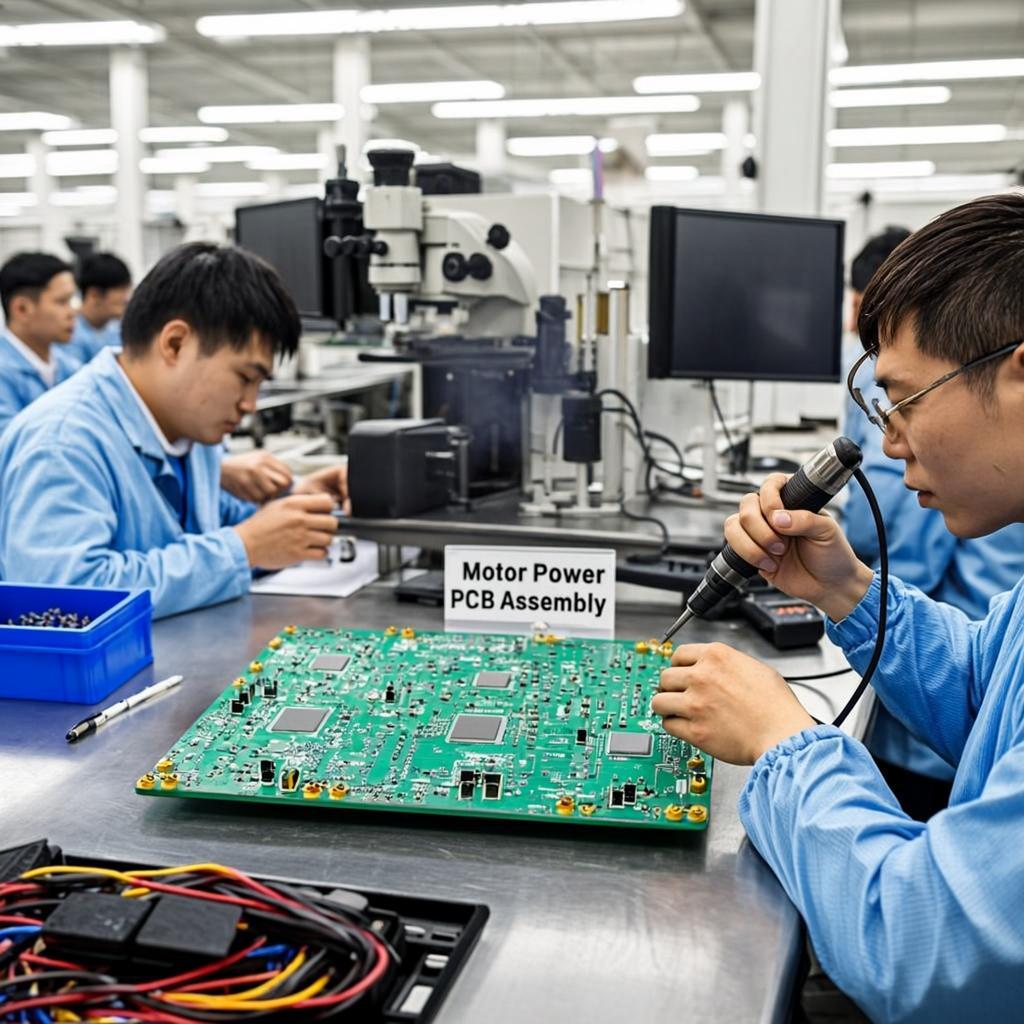
OurPCB provides end-to-end assembly services for EV charger PCBs, supporting both surface mount and through-hole technologies. SMT lines handle fine-pitch components down to 0201 packages, with placement accuracy of ±25 µm and reflow profiles optimized for multilayer high-copper boards. Nitrogen reflow is available for oxidation-sensitive assemblies, especially in high-voltage applications.
We support THT processes for connectors, relays, and large passive components using wave soldering or selective soldering with controlled thermal gradients. Double-sided reflow, mixed technology, and BGA rework services are also available. BGAs are aligned using optical centering and inspected post-process with 5 µm resolution X-ray systems.
All assembly steps follow IPC-A-610 Class 2 or Class 3 criteria, with real-time process monitoring for solder paste volume, placement alignment, and joint integrity. ESD-safe material handling, moisture-sensitive device (MSD) tracking, and batch-level lot control are standard across both facilities.
OurPCB integrates inline inspection and electrical test systems throughout the EV charger PCB assembly process to verify build quality, functional integrity, and regulatory compliance. Automated Optical Inspection (AOI) is used after solder paste printing and post-reflow to detect component skew, tombstoning, insufficient solder, and polarity errors across all SMT placements.
For assemblies with BGAs, QFNs, or embedded pads, real-time X-ray inspection validates solder joint formation and detects voids, bridging, or incomplete wetting. All BGA rework is re-inspected post-process. Solder paste inspection (SPI) verifies volume, height, and area coverage before pick-and-place.
In-circuit testing (ICT) is available for populated PCBs with accessible test points, using custom fixtures to measure continuity, resistance, diode orientation, and component presence. High-voltage testing and functional test rigs can be applied at end-of-line for charger boards operating in 220V or 380V systems. All tests follow IPC-TM-650 and customer-specific protocols for yield control and traceability.
OurPCB offers protective coating and environmental sealing solutions tailored to the outdoor and high-voltage demands of EV charger PCBs. Conformal coating, a protective film that shields against humidity, dust, and ionic contamination, is applied by selective spray, dip, or brushing methods using acrylic, silicone, or polyurethane chemistries. These coatings protect against humidity, condensation, dust, and ionic contamination, with thickness control between 25 µm and 75 µm.
We also provide three-proof treatment—moisture-proof, mold-proof, and salt-spray-proof—based on GB/T 4797.6-1995 standards. This process enhances board survivability in outdoor-rated chargers subject to IP54 or IP65 enclosures. Materials are qualified for adhesion, dielectric strength, and thermal cycling resistance.
All coated boards are UV-inspected for coverage uniformity and undergo post-cure verification before final packaging. Optional masking is available for connectors, test points, or edge fingers to maintain electrical interface integrity during the coating process.
OurPCB manufactures EV charger PCBs designed for AC, DC, and AC/DC integrated systems, supporting charger power levels from 3.3 kW up to 30 kW. We fabricate control and power conversion boards for AC Level 1 and Level 2 chargers, DC fast chargers, and bidirectional onboard modules. Each topology requires specific copper distribution, insulation spacing, and thermal design strategies incorporated at the stack-up and layout levels.
For AC designs, we support isolated control PCBs with precise routing for zero-crossing detection, relay actuation, and grid interface circuitry. DC charger PCBs are built for direct high-current transfer, with wide trace widths, heavy copper layers, and reinforced dielectric spacing to meet safety class clearance requirements.
We also support charger architectures using SiC MOSFETs, GaN FETs, and phase-shifted full bridge (PSFB), LLC, or dual active bridge (DAB) converter topologies. Our production team can adapt layer counts, thermal relief, and pad geometry to support each topology’s electrical and mechanical demands.
EV charger PCBs require substrate materials with high thermal stability, strong dielectric properties, and consistent electrical performance under load. For most AC and DC charger designs, high-Tg FR4 laminates rated to ≥170 °C prevent delamination and dielectric breakdown during continuous operation. Standard options include ITEQ IT180A, TUC TU-883, and Isola 370HR, all qualified for high voltage and thermal cycling.
For high-frequency or bidirectional power conversion modules, we select low-loss materials such as Rogers RO4003C or Panasonic R-5785 to minimize signal attenuation and dielectric heating. These materials offer low Dk drift and reduced loss tangent, supporting gate driver signals, feedback loops, and CAN/LIN interfaces in EV charger control boards.
Copper thickness is 1 oz to 3 oz for inner layers and up to 15 oz for external power planes in high-current DC output paths. To support these copper weights, we apply a thicker solder mask (eg. 15 to 25 µm dry film or 25 to 50 µm liquid photoimageable mask) to maintain electrical isolation. Solder masks conform to IPC-SM-840 Class T or H specifications, depending on coating type and required voltage.
Understanding different EV charger types helps explain the electrical, thermal, and structural demands placed on their supporting PCBs.
EV charger PCBs are used in both fixed and onboard charging systems, with design requirements that vary by deployment environment, installation method, and end-user access.
These units operate outdoors and require PCBs built with conformal coating, high-voltage spacing, and weatherproofed connectors. Power control boards manage AC grid input and drive DC output modules at levels from 50 kW to 350 kW.
Wall-mounted or portable, these systems use lower-power PCBs (3.3 to 7 kW) that focus on safety, compact layout, and efficient thermal design. EMI suppression and reinforced insulation spacing are necessary for safe operation in confined or enclosed environments.
Chargers installed in logistics yards or bus terminals require scalable PCBs designed for load balancing, vehicle authentication, and power management across multiple outputs. These boards integrate monitoring circuits and support higher duty cycles
Installed within the vehicle, these PCBs convert AC to DC internally and require compact, thermally stable designs. They must interface directly with vehicle battery systems and comply with ISO 15118 and CAN bus communication requirements.
Chat with Us
Mon-Fri: 24 hours,
Sat: 9am-6pm, GMT+8
An EV charger PCB is the primary circuit board that controls power conversion, safety interlocks, and communication between the charging station and electric vehicle. It routes high voltage and current across isolated paths, manages control logic, and interfaces with the charger’s relay, sensor, and pilot circuits.
Without a properly designed PCB, the charger cannot regulate output, meet insulation standards, or support compliant communication with the vehicle.
EV charger PCB assembly includes surface mount and through-hole component placement, soldering, inspection, and testing. SMT parts are placed using pick-and-place machines and reflow soldered in nitrogen ovens.
Power devices and connectors are wave or selectively soldered. BGAs and QFNs are X-ray inspected, and high-voltage boards are HiPot tested post-assembly. The process includes solder paste inspection (SPI), AOI, and moisture-sensitive component handling.
EV charger PCB