High-density interconnect (HDI) PCBs play a crucial role in modern electronic devices such as smartphones, laptops, medical devices, and all other high-performance devices that require complex circuitry in a small area.
HDI PCBS are a type of PCB with a higher density of wiring per unit area. HDI PCBs are designed to incorporate a large number of components in a very small area of the board. An HDI PCB has many layers connected with the help of various vias such as microvias (diameter ranging from 50-100 MM), Blind, and Buried Vias. Due to the extensive use of microvias, HDI PCBs are also known as microvia PCBs.
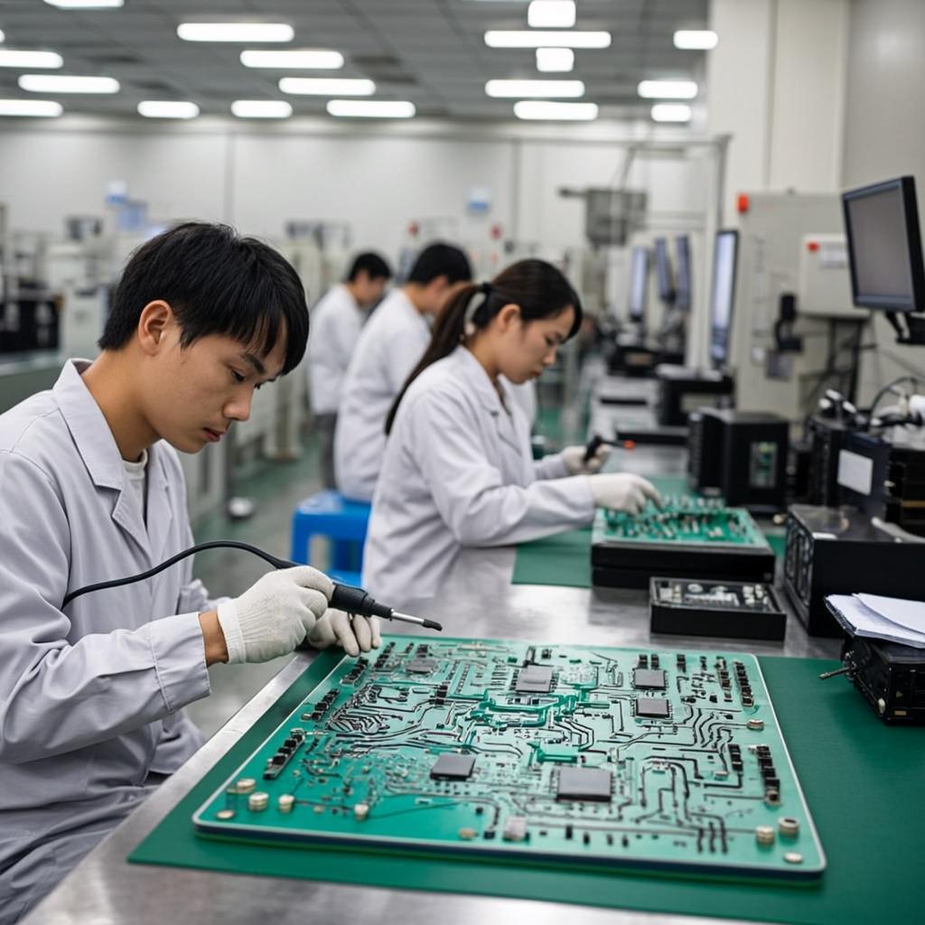
Since we have an idea of what HDI PCB is, what is its importance in modern electronics and what kind of technologies are used in making it. This article will cover the entire process of the HDI PCB fabrication from design to the production of the final product.
The design phase is crucial in the HDI PCB manufacturing process because a perfectly designed board will deliver optimum performance. There are various steps involved in designing an HDI PCB.
At the very first of the design phase all the Physical Specifications of the board are analysed this analysis includes:
Different materials for HDI PCB electronics manufacturing are analyzed at this stage based on performance, reliability, and manufacturability. Choosing the right material for the substrate and laminate is very crucial as their selection is based on many factors the following table describes different HDI PCB materials.
A detailed diagram of all the electrical connections and footprints for placing the components is created at this stage on CAD software. TinkerCAD, KiCad, and EasyEDA are the most popular software for creating the schematic design of PCBs. To validate this schematic diagram electrical rule check should be applied to it.
Deciding the number of layers in a HDI PCB is very crucial in the design phase. An HDI PCB consists of multiple layers usually in a Stackup configuration of 4, 6, or 8 layers. These layers contain power planes, ground planes, and signal layers. All the layers should be balanced otherwise the PCB will wrap during the fabrication process. To prevent electromagnetic interference all the layers should be adjacent to each other. Thermal management should also be considered in layer stackup design as the power plane and ground plane can dissipate heat which maintains the temperature of the PCB.
Maintaining signal integrity is very crucial in HDI PCBs. In HDI PCB design, selecting types of vias (microvias, blind vias, buried via