High-density interconnect (HDI) represents the cutting edge of the printed circuit board industry today, due to the demand for signal integrity and compact circuit boards. But do you master HDI board design like you should?
In our previous article series becoming a PCB design master, we have focused on designing for circuit board assembly and achieving faster time to market. This article will hone in on the finer points designers must know in order to master HDI boards.
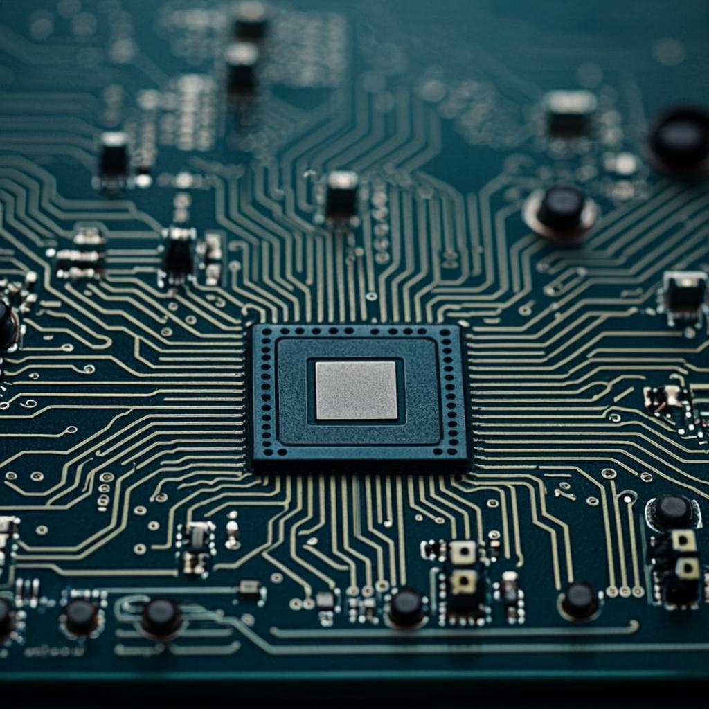
HDI boards feature higher wiring density per unit surface area than standard boards. HDI use some or all the below features that reduce the size of the board:
The increased interconnection density allows for enhanced signal strength and improved reliability. Additionally, thanks to design efficiency and space maximization, HDI boards make it possible to manufacture smaller, more powerful electronic devices.
Why is there even a separate category of board technology called HDI? Well, when the lines get smaller than 65 microns (2.559 mils), the ability to etch your trace and space is diminished. You can’t really use a traditional etching process. For example, typical etching on a standard board allows for a very thick resist along with standard imaging on an LDI machine and you essentially have plenty of space for any tolerances needed to etch those spaces. In a microelectronic environment, you don’t have any of those leeways. The features are so close together that traditional etching processes don’t work.
HDI technology is the best choice for board designers when they require a higher density of components. So what makes HDI different from the standard board? Mainly three things:
HDI uses microvias instead of through-hole vias where higher precision is required. Laser drilled microvias can be used up to a drill hole depth of approx 100µm. Since microvias have a short barrel they do not face problems with different CTE (coefficient of thermal expansion) values of substrate and copper. That’s why microvias are more suitable than through-hole vias.
The best practice for designing an efficient HDI is to replace the most common vias (blind, buried, or through-holes) with microvias. Move the most commonly used layers (Ex: GND or PWR) to the top of the stack-up if they don’t have components and traces on them (GND and PWR planes need to be solid and unbroken). This stack-up arrangement can either eliminate the vias required or allow to replace the through-holes with microvias. As the microvias don’t go throughout the thickness of the board, this provides more space on the other layers. Hence, this practice can improve the routing density of the inner layer and reduce the number of signal layers.
Different stack-up arrangements are used in the HDI structure to reduce the number of through-holes and the number of inner layers. The ground and power planes are the most used layers to drill vias. HDI PCB designers can reduce the number of stack-ups by placing these layers at the top of the stack-up, say layers 2 and 3. The top and bottom layers are normally used for component placement.
Three examples of HDI stack-up
Thin dielectric layers less than 0.005 inches are used to separate GND and PWR planes. This provides a low power supply impedance and also enables the use of ‘skip vias’ from layer 1 to layer 3.
Proper arrangement of vias is crucial in HDI board designing. The arrangements aim at providing better signal integrity and improving routing space in the inner layers. Here’s a depiction of stacked vias:
Stacked vias
Fine-pitch BGAs create a necessary complication with HDI where the design rules are chosen to not provide clearance for staggered blind vias. The stacking of two microvias or placing a microvia on top of the buried via is needed when this situation arises.
Blind vias are arranged to form a boulevard structure. Boulevard formation can reduce the total number of power layers and doubles up the routing space.
Boulevard arrangement
These structures can be created by skip vias, multiple buildup, or sequentially laminated, and laminated vias. It is also used for routing of high-speed critical nets using only the cross-over from horizontal to the vertical connection of small and low inductance blind vias.
In the past, high-density interconnect has run up against the wall of board technology. And today, with lots of innovation and investments, we are able to push the boundaries of circuit board fabrication when it comes to trace widths and spaces. So HDI PCB design is essentially defined by the spaces between traces as well as all copper features. In that regard, we want to define HDI and microelectronics and provide a few suggestions to you on understanding design rules and how they interplay with each other to get a good design.
For a thorough understanding of HDI architecture, we are obligated to provide you the information on the basics. First, we’ll check out possible stack-up structures and then discuss how to approach the manufacturer with the design idea.
Before we discuss HDI designing and design rules in detail, we would like you to get accustomed to the standards that govern HDI PCB design.
IPC/JPCA-2315: Design guide for high-density interconnect structures and micro vias.
IPC-2226: Standard specifications for material characterization, microvia formation, interconnecting structure, and selection of design rules.
IPC/JPCA-4104: This standard helps in identifying the material required for the HDI structure. Qualification and performance specification for dielectric materials for high-density interconnect structures.
IPC-6016: Contains general specifications for the high-density substrate. Qualification and performance specification for HDI structures.
Let’s look at the basic structures of HDI PCB technology before discussing the design rules and the other aspects. The two basic HDI structures that exist are the “buildup”/ “sequential lamination” and the “any-layer” structures.
The build-up structure is the most commonly used type of HDI structure. The sequential lamination process is used to build this structure. Cores are constructed and laminated first, then drilling, plating, and filling in this plane is done. After this process, this layer is laminated with other layers, and the drilling, plating, and filling processes repeat.
According to IPC 2226 standard, HDI structures are classified into six types:
Let us check the basic structures of sequentially laminated HDIs.
1+N+1
In the 1+N+1 type of stack-up, ‘1’ represents one sequential lamination on either side of the core. One sequential lamination adds two copper layers for a total of N+2 layers. There is one extra lamination on the top layer and stacking of the vias is allowed. This buildup is suitable for BGA with lower I/O counts and its mounting stability is excellent.
2+N+2
Now, check the 2+N+2stack-up shown above. This buildup contains 2 layers of high-density interconnection, suitable for BGA with smaller ball pitch and higher I/O counts. These designs use copper-filled staggered or stacked micro vias that are commonly used in high-level signal transmission applications.
The “Any-layer”structure is another approach used in HDI PCB design. Any-layer boards are the next-level advancement in HDI that follows the type VI HDI standard. Any-layer technique is used for high-level interconnection applications because all of the microvia layers can be freely interconnected.
Any layer structure in HDI
In this method, microvia layers are used as redistribution layers in the prepreg or we can say they are floating in prepregs. Microvia in a layer is constructed first, following the process of drilling, filling, plating, printing, etching, and lamination. Then, other layers are stacked above the existing layer following the same process.
The number one question designers usually ask is… what pad sizes, what hole sizes and how tight can the traces and spaces be together? These are good questions as long as you’re designing a relatively standard board. You can’t just look at our HDI PCB manufacturing capabilities page and not understand how they interact with each other. For standard products, it may work, but as you get into more complicated boards such as HDI or microelectronics with finer feature sets, it may not work.
Let’s say you’re doing an HDI construction with very fine lines and you are going to do, let’s say a 2+4+2 type of stack-up. So 2+4+2 essentially means you’re going to have a buried sub-construction which we will mechanically drill and plate. Now, if we have to do fine lines on layer 3 of the buried sub-construction, that becomes problematic. The processes on layer 3, don’t allow for fine line technology. Whereas on layer 2, you have more leeway for your fine lines.
2+4+2
Now when you get into that feature set, designing the whole board with those feature sizes is not the same as designing just a small portion of the board with those feature sets. If you can loosen up the spacing with bigger pad sizes and bigger drill sizes in non-dense areas it will make it easier for the manufacturer and less costly for you… especially if you’re going into production.
So we really wanted to dive deep on that distinction. Even though our capabilities would say 35 microns is the minimum trace and space, it is not a feature size that we would recommend or be able to manufacture across the entire design.
“Increased interconnection density allows enhanced signal strength.”
Higher density means HDI designers must constantly keep layout and spacing in mind, among other factors. The following are four tips on avoiding common HDI board design mistakes.
Considering space during HDI PCB design means more than squeezing in as many components as possible. First, designers must ensure boards can be properly maintained in the future. Determining the amount of space between specific components and opting for an extra room is a requirement. This can also make things simpler during board manufacturing. Via diameter, pad diameter, and trace width should all be taken into account before implementation begins. Otherwise, circuit boards may have to be completely redesigned, requiring further time, money, and energy. Read our case study on designing 8 and 14-layer HDI PCBs with stacked vias to learn the techniques we implemented to build reliable stacked microvias.