High-frequency pcb design affects how wireless pcb works in smart homes. Each wireless pcb links modules for Wi-Fi, Zigbee, and Bluetooth. Engineers know that wireless pcb choices affect communication and range. They also affect how modules fit together. A wireless pcb must work with many wireless modules. It must also support iot applications. Small pcb layouts help smart devices use less space. Designers care about wireless communication and high performance. They want all modules to work well. Good wireless pcb design stops interference. It also helps internet of things applications work better. Smart applications need wireless pcb solutions for EMI and EMC. Learning wireless pcb and module design makes stronger devices. It also helps make modules ready for the future.
Smart homes use wireless technologies to link devices. Wi-Fi, Zigbee, and Bluetooth each have special features for iot. Wi-Fi lets many devices send data fast on the network. Zigbee uses less power and builds a mesh network for smart modules. Bluetooth helps devices talk to each other over short distances.
Wi-Fi modules move lots of data for smart devices. Zigbee modules save power and connect many devices together. Bluetooth modules give strong wireless links for personal gadgets and smart tools.
Tip: Using Wi-Fi, Zigbee, and Bluetooth together helps smart homes. This way, wireless signals reach more places and support more iot uses.
Wireless modules use different rules and bands to send data. Wi-Fi works on 2.4 GHz and 5 GHz bands. Zigbee uses the 2.4 GHz band for mesh networks. Bluetooth also uses the 2.4 GHz band for safe data sharing.
Wireless tech needs to handle many rules at once. Built-in wireless modules let smart devices switch between Wi-Fi, Zigbee, and Bluetooth. This makes iot work better. Engineers design wireless PCBs to stop signal problems and help data move faster. They pick modules that fit what smart devices need.
Wireless modules are important in smart home networks. They help send data fast and keep connections strong. Multi-protocol support lets smart devices share data using different wireless tech.
Engineers pick multilayer pcb designs for smart home gadgets. These designs have four or more layers. Each layer helps with tricky wireless pcb layouts. Multilayer pcbs are good for high-frequency pcb needs. They make it easier to route wireless signals. More layers let engineers split power and ground planes. This split cuts down on noise and stops interference in wireless communication.
A multilayer pcb also saves space in devices. Smart home gadgets need small boards. Multilayer designs let engineers put many wireless modules on one pcb. This helps everything work together and makes the wireless pcb stronger. Devices can use Wi-Fi, Zigbee, and Bluetooth all at once. Multilayer pcbs also help control heat. Good heat control keeps wireless modules working longer.
Note: Multilayer pcbs help manage signal paths. This makes wireless work better and keeps signals from getting lost.
Impedance control is very important in high-frequency pcb design. Each trace on the pcb must match the impedance of the wireless module. If impedance does not match, the signal can bounce back. This bounce causes loss and weakens wireless communication.
Signal integrity means keeping signals strong and clear. Engineers use special layouts to stop signals from crossing or mixing. They keep traces short and straight. This helps the wireless pcb send and get data without mistakes. Good signal integrity means the wireless module can talk to other devices without trouble.
Here is a table with ways to make signal integrity better:
Wireless communication needs strong signals. Engineers test the pcb to make sure signals stay safe. They use tools to check for signal loss and fix problems before making the final wireless pcb.
EMI means electromagnetic interference. EMC stands for electromagnetic compatibility. Both are big problems in wireless pcb design. EMI can come from other electronics or even from the same pcb. Too much EMI can block wireless signals or cause mistakes.
Engineers use tricks to lower EMI. They add ground planes in the pcb. These planes soak up bad signals. They also use shielding to protect important parts of the wireless pcb. Placing parts carefully helps too. Keeping noisy parts away from wireless modules makes wireless communication stronger.
Tip: Always test the wireless pcb for EMI and EMC before using it in smart home gadgets. This testing helps stop problems with wireless signals later.
Smart home gadgets need strong wireless communication. Good EMI and EMC design keeps the wireless pcb working well. It also helps the device pass safety tests and work in many homes.
Zigbee uses the 2.4 GHz band. It lets smart home devices talk to each other. Many engineers pick zigbee because it does not use much power. This helps sensors and lights last a long time. Zigbee can make a mesh network. Each zigbee module can send messages to other modules. The mesh network lets signals reach all parts of the house. Zigbee design tries to save energy and keep connections strong.
Smart home devices use two main antennas with zigbee. The first is the PCB antenna. Engineers put this antenna right on the circuit board. PCB antennas are small and cost less money. They work well in small zigbee devices. The second is the omnidirectional antenna. This antenna sticks out from the device. It sends signals in every direction. Omnidirectional antennas can give zigbee modules a longer range.
Note: PCB antennas are best for zigbee designs where space is tight.
Engineers must put the zigbee antenna in a good spot. Good placement helps the zigbee module send and get signals well. They keep the antenna away from metal and noisy circuits. This stops interference and keeps the signal strong. Many engineers use a ground plane under the zigbee antenna. This makes the antenna work better. They also test the device in real homes to check the signal.
Here are some tips for better zigbee antenna placement:
Zigbee helps smart homes by using little power and strong mesh networks. Picking the right antenna and putting it in the best spot makes zigbee work even better.
Engineers split the wireless pcb into different sections. They keep analog, digital, and wireless parts apart. This stops noise from moving between sections. Each part does its own job. The wireless part handles sending and getting signals. The analog part works with sensor signals. The digital part controls data and logic.
Splitting up the pcb helps stop interference. Engineers use ground planes to keep sections apart. They put the wireless module away from noisy digital parts. This keeps the wireless signal safe and clear. Good isolation helps the wireless pcb pass EMC tests.
Tip: Put the wireless part close to the antenna edge. This helps keep signals strong and makes wireless work better.
Trace design is important for wireless pcb performance. Engineers make traces short and straight. Short traces lower resistance and keep signals strong. Wide traces help send high-frequency signals. They also help stop the pcb from getting too hot.
Engineers pick trace width to match the needed impedance. Controlled impedance keeps signals clean. They use smooth curves instead of sharp corners. Smooth curves help fast signals move better. Engineers use microstrip or stripline methods for good signal quality.
Here is a table with trace design tips for wireless pcb:
Engineers test the pcb for signal loss. They use tools to check if signals are strong enough. Good trace design helps the pcb work with Wi-Fi, Zigbee, and Bluetooth.
Interference can make wireless pcb work badly. Engineers use many ways to lower interference. They add ground planes under the wireless part. Ground planes block noise and keep signals safe. Shielding covers important parts of the pcb. This keeps outside noise away from the wireless module.
Engineers space out transmission lines on the pcb. This stops signals from mixing together. They keep power and ground lines away from wireless traces. Careful part placement helps lower interference. Engineers use filters to clean up power for the wireless part.
Here are some steps to lower interference in wireless pcb:
Note: Testing the wireless pcb in real life helps find and fix interference before making the final product.
Engineers work hard to lower interference and keep signals strong. A good wireless pcb helps smart home devices send and get data without problems.
Smart home devices must follow RF compliance rules. These rules make sure each wireless pcb is safe. They also help stop problems with other devices. Engineers test the wireless pcb to see if it meets standards like FCC or CE. They measure how much energy the wireless pcb sends out. They also check if the signals stay in the right frequency bands.
Special tools are used for RF compliance testing. Engineers put the pcb in a test chamber. They use antennas to measure the signals. If the wireless pcb does not pass, engineers change the design. They might add shielding or move parts around. Passing RF compliance tests lets smart home devices work in many countries.
Note: RF compliance testing keeps users safe. It also helps protect wireless networks from interference.
Engineers test the signal and power of each wireless pcb. They check if the signals stay strong from the module to the antenna. Tools like spectrum analyzers help them see if signals are clear. Weak or noisy signals can make smart home devices lose connection.
Power testing checks if the pcb gives the right voltage and current. Too much or too little power can hurt the wireless pcb. It can also make it stop working. Engineers use multimeters and oscilloscopes for these tests. They look for drops or spikes in power that could cause problems.
A simple checklist for signal and power testing:
Good testing helps engineers find problems early. This makes the wireless pcb work better in smart home devices.
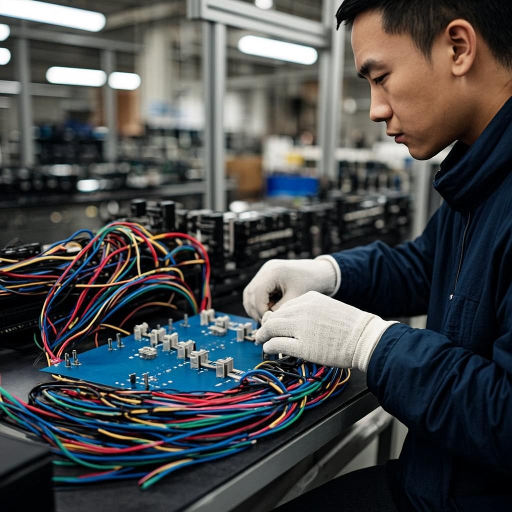
Engineers have problems when putting together wireless modules for iot. They need to be careful with each pcb. This keeps wireless parts safe from harm. Clean workspaces are important for good assembly. Dirt or dust can block signals in wireless devices. Engineers use antistatic tools to protect zigbee and other modules from static electricity.
They check every connection on the pcb during assembly. Loose parts can make wireless signals stop working. Magnifiers help engineers find tiny problems. If a wireless module fails, they test the power supply first. Weak power can stop iot applications from working. Signal testers help check if the wireless module sends and gets data.
Troubleshooting means looking for broken traces or antennas. Engineers swap out bad parts and test the pcb again. They write down each fix to help with future repairs.
Tip: Test wireless devices in real iot applications before using them. This helps find hidden problems early.
Smart home technology c