Conventional printed circuit boards serve as the backbone of basic electronic design, but as device complexity, miniaturization, and performance demands rise, high density interconnect (HDI) PCBs become a necessary upgrade. HDI technology leverages Sequential Lamination, microvias, and fine-pitch routing to solve the limitations of traditional boards, with compliance to IPC standards (IPC-2226, IPC-6012) ensuring reliability and manufacturability. Below is a structured breakdown of the core scenarios where HDI PCBs are the only viable solution, paired with technical specifics, industry benchmarks, and practical comparisons to guide design, procurement, and fabrication decisions.
Miniaturization is the primary driver for HDI adoption, as consumer and industrial electronics demand more functionality in smaller form factors—an objective conventional PCBs cannot achieve due to their larger via sizes and lower routing density. HDI PCBs deliver 2–3x higher circuit density in the same physical area, making them indispensable for compact device design.
The table below quantifies the space efficiency gap between HDI and conventional PCBs for miniaturized designs:
HDI is non-negotiable for devices where physical size is a hard constraint: wearables (smartwatches, fitness trackers), implantable medical devices (pacemakers), portable consumer electronics (smartphones, true wireless earbuds), and compact industrial sensors. For procurement and design teams, this means eliminating the need for multiple conventional boards in a single device—one HDI board integrates all functionality, reducing assembly complexity and device weight by up to 40%.
Signal Integrity is the cornerstone of high-speed/high-frequency design, and conventional PCBs introduce critical flaws (via stubs, parasitic capacitance, crosstalk) that degrade signal performance at frequencies above 2GHz or data rates above 10Gbps. HDI PCBs are engineered to minimize these issues, making them the standard for 5G, RF, AI, and data center applications.
For engineers designing high-speed systems, HDI resolves the common pain point of balancing speed and manufacturability: conventional PCBs require costly back-drilling to remove via stubs, while HDI’s microvia technology achieves stub-free routing natively. This reduces fabrication time by 20–30% and eliminates back-drilling-related defects (e.g., incomplete stub removal).
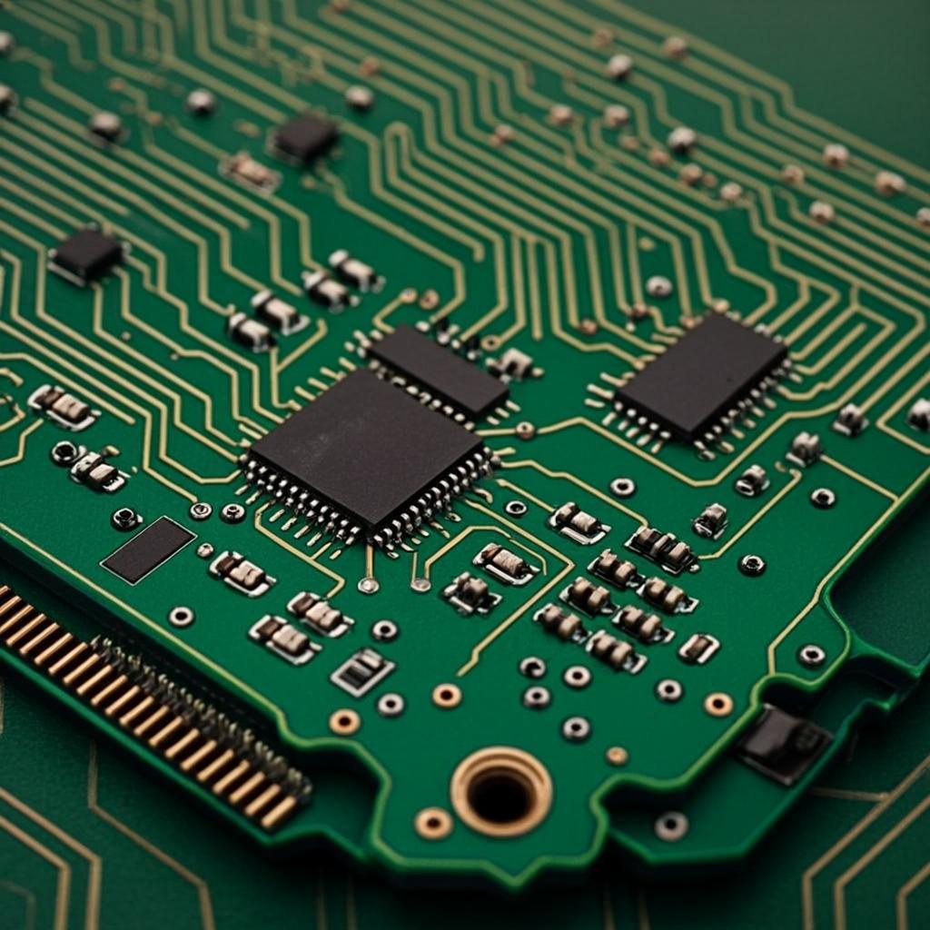
Fine-pitch ball grid array (BGA) components (pitch ≤0.65mm, and ultra-fine pitch ≤0.4mm) are ubiquitous in modern electronics, but conventional PCBs lack the routing density to fan out these components without layer count bloat. HDI PCBs use microvias and via-in-pad (VIP) technology to enable efficient BGA fanout, a capability that directly addresses the design pain point of routing congestion.
A common design challenge is layer count reduction: a conventional PCB for a 0.4mm pitch BGA requires 10–12 layers for fanout, while an HDI PCB achieves the same fanout with 6–8 layers (Sequential Lamination), reducing material costs by 25–30% despite higher HDI fabrication per-layer costs.
Modern electronics demand the integration of diverse components (ICs, passives, sensors, RF modules) on a single board, and conventional PCBs fail here due to low routing density and fixed layer stackups. HDI PCBs enable high component density through flexible stackup design and efficient use of inner/outer layers, solving the procurement and design pain point of multiple board assemblies (MBAs) in compact devices.
HDI PCBs achieve a wiring density (inches of trace per square inch) of 200–400, compared to 50–100 for conventional multi-layer PCBs. This metric, a key industry benchmark, quantifies HDI’s ability to integrate more functionality in the same space—critical for procurement teams evaluating board efficiency.
High component density and miniaturization create heat concentration in electronic devices, and conventional PCBs have poor thermal dissipation due to thick dielectric layers and sparse via placement. HDI PCBs address this pain point with optimized copper distribution and thermal via design, ensuring reliable operation in high-power, space-constrained systems.
In compact high-power designs (e.g., a 10W wearable sensor), an HDI PCB reduces component junction temperature by 15–20°C compared to a conventional PCB of the same size, extending component lifespan by 2–3x (per the Arrhenius equation for electronic reliability).
Conventional PCBs fail in harsh environments (extreme temperatures, vibration, humidity, mechanical stress) due to their large through-hole vias (high aspect ratios, weak plating) and rigid stackups. HDI PCBs, built to IPC-6012 Class 3 and automotive IATF 16949 standards, deliver superior reliability by design, solving the critical pain point of field failure in industrial, automotive, aerospace, and military applications.
HDI PCBs for harsh environments must comply with:
For quick reference, the table below summarizes the core scenarios, technical capabilities, and cost tradeoffs that define the choice between HDI and conventional PCBs—an essential tool for design engineers and procurement teams: