High density interconnect (HDI) PCBs enable denser routing, finer lines and spaces, smaller vias, and more layers than conventional PCBs. They are essential for miniaturized and high performance electronics like smartphones, wearables,IoT devices,automotive electronics, and medical devices.
Selecting the right HDI PCB manufacturer is crucial to get high yields, quality, and timely delivery for prototyping and volume production. This article provides a comprehensive list of the top 18 HDI PCB manufacturers across the globe along with a framework for comparing their capabilities and selecting the optimum partner.
HDI refers to the use of microvias (smaller than traditional vias) to interconnect layers in a PCB. This allows greater routing density. Some key features:
Benefits of HDI technology:
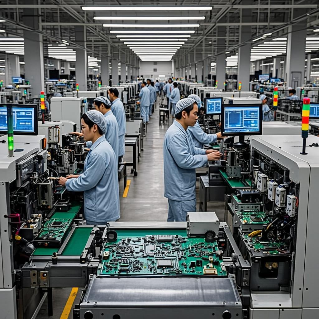
HDI PCBs require specialized manufacturing processes and equipment. Not all standard PCB manufacturers have HDI capabilities.
AT&S is Europe’s largest PCB manufacturer and a leading global producer of HDI boards and IC substrates. The Austria-based company operates plants in India, China, Korea, and Austria.
Key capabilities for HDI PCBs:
AT&S focuses on high-end PCB technologies for applications like 5G equipment, automotive radar, and advanced driver assist systems (ADAS). Other areas of expertise include automotive, industrial, and medical PCBs.
Tripod Technology is one of the largest PCB manufacturers in Taiwan with revenues of over $1 billion. The company has HDI capabilities across multiple facilities:
Tripod specializes in producing ultra-thin, high-precision HDI boards using MSAP for customers serving the communications, networking, automotive electronics, and consumer wearables segments.
3rd floor, Building D, Baishixia Industrial Zone, Jian 'an Road, Fuhai Street, Bao 'an District, Shenzhen, China.
MAGIC Certifications
Delivery
© 2024 Magic Electronics Tech Ltd. All Rights Reserved