ENSURING THE HIGHEST STANDARDS OF QUALITY AND SAFETY Why us for consumer electronics PCB
At KKPCB, we combine advanced technology with industry best practices to deliver even the most complex PCBs. Our expert team ensures excellence at every stage — from design to assembly — guaranteeing precision, reliability, and performance.
At KKPCB, we strictly follow industry standards and best practices to deliver reliable PCBs for consumer electronics. With rigorous testing protocols in place, we eliminate errors and ensure consistent quality and performance.
In the fast-paced consumer electronics market, speed is everything. At KKPCB, we provide quick turnaround times to help you accelerate product launches and stay ahead of the competition.
At KKPCB, we accommodate all production needs — from small prototype quantities to large-scale manufacturing. No matter the volume, we ensure high-quality PCBs with consistent performance and reliability.
KKPCB offers extensive PCBA, wire harness, cable, and box build assembly services for commercial and industrial markets, with a strong focus on the electric vehicle industry. Our experienced team works with customers to fully realize their electric vehicle designs, regardless of the complexity.Automotive electronics is the combination of electronic information technology and traditional automotive technology. It is the general term for body electronic control and vehicle electronic control. PCBs are widely used in automotive electronics, including power control systems, safety control systems, body electronic systems, entertainment communications, etc.
At KKPCB, we provide complete manufacturing solutions for audio devices, from PCB design and prototyping to assembly and testing. Using rigid, flex, and rigid-flex PCBs, we ensure high performance, reliability, and superior sound quality for headphones, speakers, home audio, and professional audio equipment. With advanced processes and strict quality control, we help clients accelerate time-to-market while delivering flawless audio electronics.
KKPCB provides consumer product electronics manufacturing services covering all stages of product development. Includes PCB design and manufacturing, prototyping, testing, assembly and packaging. Our expertise ensures seamless execution of projects from concept to delivery.
At KKPCB, quality and reliability are at the core of our operations. We follow strict quality control measures and comply with all industry standards and regulations to ensure every PCB meets or exceeds customer expectations. Our commitment is reinforced by global certifications, including ISO 9001, ISO 13485, ISO 14001, IATF 16949, REACH, UL, and PDA, guaranteeing that our products deliver superior performance, safety, and consistency across consumer electronics, automotive, medical, and industrial applications.
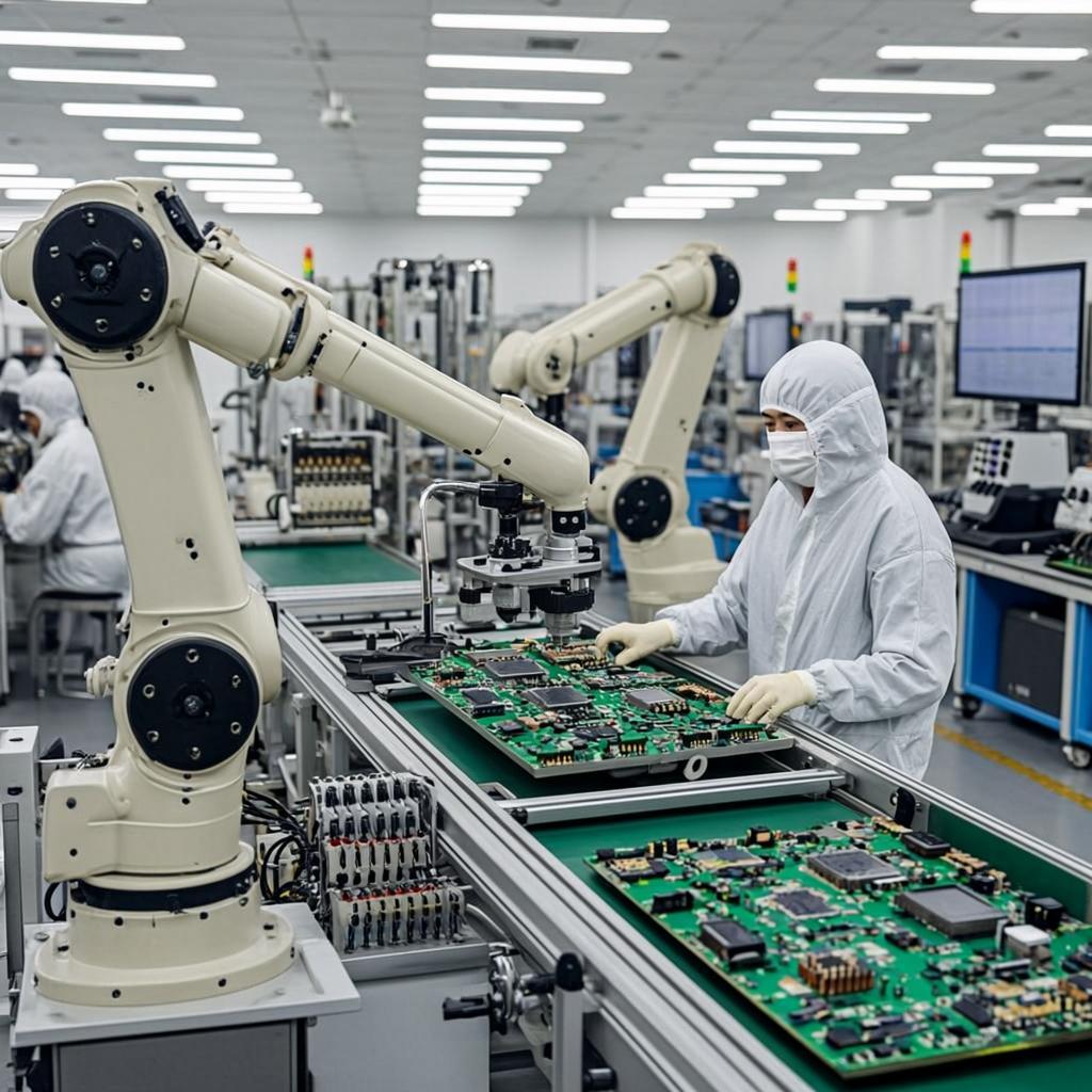
At KKPCB, our consumer electronics PCB manufacturing process is designed to ensure precision, reliability, and high performance at every stage. We begin with PCB design and layout, optimizing for electrical performance and manufacturability. Next, we move to prototyping, allowing for rapid testing and validation of designs. Once approved, the PCBs undergo high-quality fabrication using advanced materials and processes, followed by component assembly, soldering, and inspection. Throughout production, we employ rigorous testing protocols, including functional testing, AOI (Automated Optical Inspection), and electrical testing, to guarantee every board meets strict quality standards. Finally, the PCBs are packaged and shipped, ready for integration into consumer electronics such as smart home devices, wearables, portable gadgets, and audio systems.
To begin with, a PCB layer is created using a PCB design software by designers. Once the design is approved for production, the design is exported into a supportive format. A Design for Manufacturability test is run to ensure that the design fulfills the requirements for minimum tolerances. What follows next is the PCB printing process.
The film is next printed onto a copper foil. The basic form of PCB is a laminate board whose core material is epoxy resin and glass fiber. The laminate serves as an ideal body for receiving the copper. The substrate material provides a sturdy and dust-resistant starting point for the PCB. Copper is pre-bonded on both sides. The process involves whittling away the copper to reveal the design from the films.
sided laminate is cleaned and the clean panel receives the photo resist layer, which hardens after exposure to UV light. The light passes through the clear parts of the film, hardening the photo resist on the copper underneath. The areas not meant to harden are then slated for removal.
A powerful chemical preparation is used to eat away the excess copper. While the exposed copper is removed, the desired copper remains protected beneath the layer of photo resist.
The inner layers are now aligned to the outer ones. With the help of an optical punch, holes are accurately punched. An Automatic Optical Inspection is carried out to ensure absence of defects. Once the stage of inspection is passed, the PCB moves to the final stages of production.
All the layers are now fused. A prepreg layer is placed over the alignment basin. The substrate layer fits over the prepreg before placing the copper sheet. More sheets of prepreg sit on top of the copper layer. Finally, an aluminum foil and copper press plate complete the stack. Now it’s prepped for pressing.
Holes are now are bored into the stack board. An x-ray locator identifies the drill target spots.
After drilling, the panel moves onto plating. The process fuses the different layers together using chemical deposition. After a thorough cleaning, the panel undergoes a series of chemical baths.
Photo resist is once again applied and exposed to UV light. Finally, the outer plates undergo inspection to ensure all of the undesired photo resist was removed.
The panel is electroplated with a thin copper layer. Etching removes the unwanted copper foil from the panel.
The unwanted copper undergoes removal. The tin protects the copper during this stage.
Panels are cleaned and solder mask applied to both sides and exposed to UV light. The covered portion remains unhardened and undergoes removal.
The appropriate surface finish is added based on bespoke requirements and based on the environment under which the electronic product has to operate. At Mer-Mar Electronics, we have a wide range of surface finishes on offer.
The vital information pertaining to the PCB is next written on the surface.
Electrical tests are next performed to check functionality. At Mer-Mar Electronics, we also perform the Flying Probe Test to test the electrical performance.
Printed Circuit Boards are now cut from the original panel. This is done using a Router or V-Groove.
At KKPCB, the following are our capabilities when it comes to Consumer Electronics PCBs:
Consumer Electronics PCBs find extensive application in a wide range of products including but not limited to:
What is Consumer Electronics PCB?
What are the PCB assembly development trends for consumer electronic products?
The most advance trends of consumer PCB electronic products are miniaturization and diversification. There are many other trends as well including integrated circuits development, passive and discrete devices, substrate board, environmental protection awareness and more.
What are some of the change consumer electronics PCBs are undergoing?
Do you undertake DFM services for consumer electronics?
Do you have a robust testing regimen for consumer electronics PCB?
How does one get a quote for consumer electronics PCBs from KKPCB?
Can you handle complex electronics PCB designs with multiple layers?
Do you offer a choice of finishes for consumer electronics PCB assembly?
Yes, the choice of finish is recommended basis the environment the PCB has to work in.
Can l count on you for a quick turnaround time?
Can you handle all volume requirements for consumer electronics circuit board?
Can l count on you for cost-effective consumer electronics PCB quotes?