Seeking for PCB fabrication specifications? This guide covers all critical aspects from material selection to final panel dimensions for reliable PCB manufacturing.
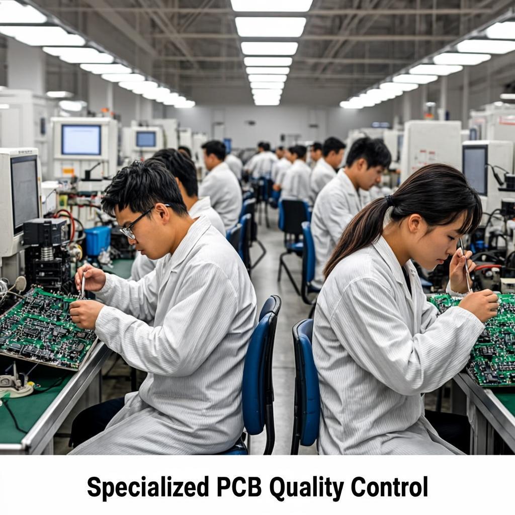
With 18+ years of PCB manufacturing expertise, EBest Circuit (Best Technology) delivers reliable solutions through standardized production processes, every operation follow PCB fabrication specifications to ensure consistency. Our advanced manufacturing capabilities support all surface finishes (ENIG, OSP, immersion silver/tin) and specialty boards including HDI (up to 20 layers), RF (controlling εr ±0.2), and heavy copper board (6oz+). Competitive pricing with transparent cost structures eliminates hidden fees, while 100% batch inspection guarantees defect rates below 500ppm. We can achieve 24-hour prototype turnaround (from Gerber to shipment) and volume production lead times 30% shorter than industry averages, enabling clients to accelerate time-to-market. For high-mix applications from 5G antennas to industrial controllers, our engineering team resolves fabrication challenges through adaptive process optimization. Welcome to contact us for a quote now: pcb@frankenthalerfoundation.org.
PCB fabrication specifications define the precise technical requirements for manufacturing printed circuit boards, encompassing material properties, dimensional tolerances, processing methods, and quality validation criteria. These specifications document essential parameters such as laminate material grades, copper weight tolerances (typically ±10%), drilling positional accuracy (±0.05mm standard), plating thicknesses (25μm minimum for through-holes), solder mask application standards (15-25μm LPI thickness), and surface finish requirements (e.g., ENIG with 3-5μm nickel layer). They establish testing protocols including impedance control verification (±10% tolerance), microsection analysis for plating quality, and IPC Class 2/3 acceptance criteria for visual defects. The specifications also address panelization rules (V-cut depth tolerances), environmental conditioning procedures (thermal stress testing), and final packaging standards (moisture barrier bags with desiccant). By systematically defining these manufacturing parameters, PCB fabrication specifications ensure consistent production quality while maintaining compatibility with assembly processes and end-use operating conditions.
Below are substrate for PCB fabrication specifications :
Copper foil thickness and tolerance of PCB fabrication specification:
Drilling and routing tolerances of PCB fabrication specification:
Here’s a practical breakdown of plating thickness standards:
Here are the solder mask for PCB fabrication specifications presented in clear:
Surface Finish Requirements for PCB Fabrication: