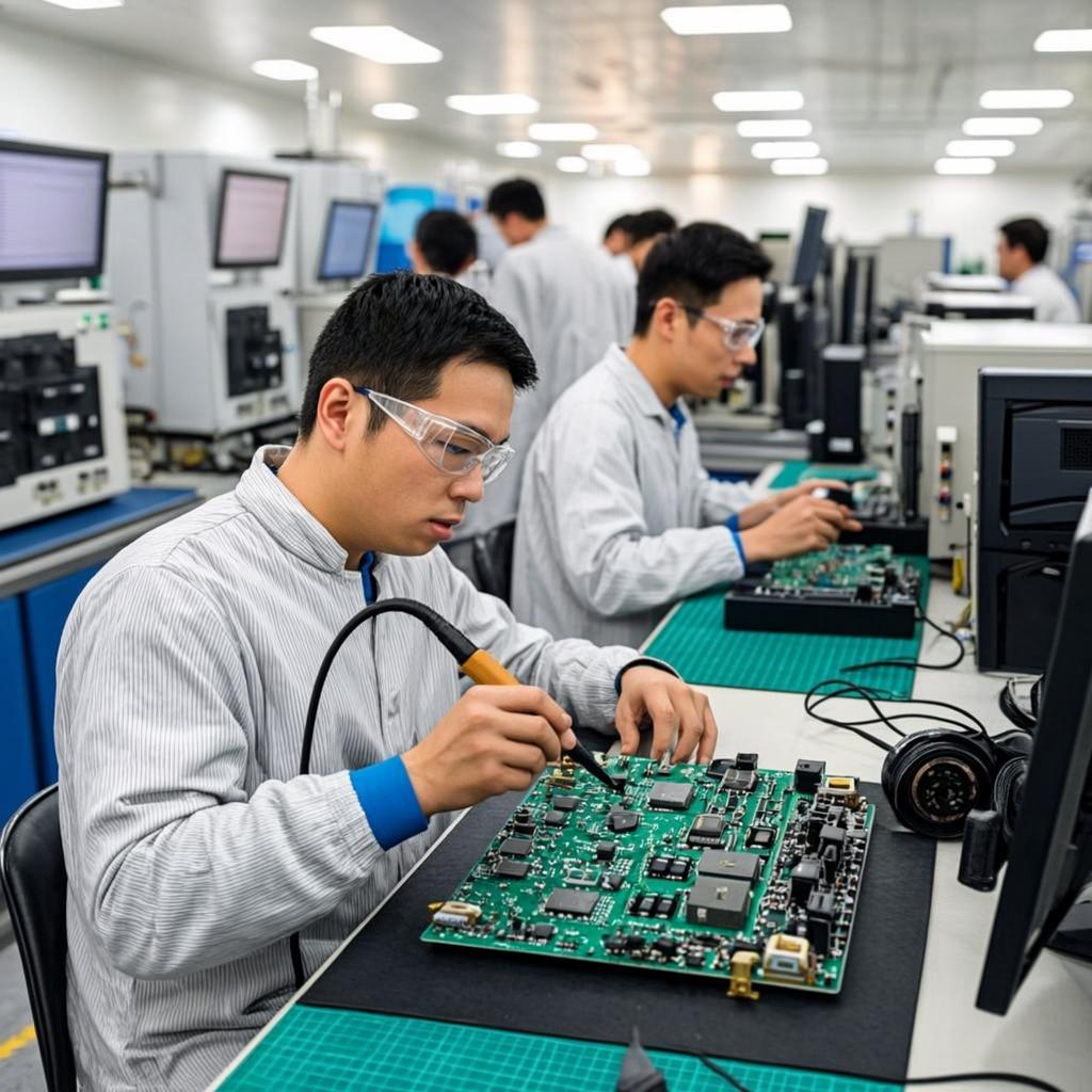
In PCB and Cu-Flex keypad’s construction, flexible or rigid printed circuit board (PCB) is base.
The printed circuit board (PCB) consists of an insulating material on which paths and solder pads are located. It is made with an etching technique. Glass-epoxy laminate or a composite material are coated with copper. Electrical connections are printed and then further processed. The structure can consist of one, two or more layers. The components are assembled on the PCB in two ways: THT (through hole technology) or SMT (surface mount technology). The plate can be the keypad’s back panel at the same time.
The flexible printed circuit (Cu-Flex) is made of a dielectric material, usually a polyimide or polyester film, on which electroplated copper conductive tracks are printed, insulated on both sides. The flexibility of the circuit depends on the material used and the number of layers. Thickness usually oscillates between 12 and 125 μm. The thicker the circumference, the stiffer it is, which affects the smaller deformation.
The advantage of Cu-Flex is its small thickness, easy adaptation of the tile to the shape of the enclosure.
The use of a printed circuit in the construction of the keypad allows placing beside contact fields and other electronic components. Additionally, there is a possibility of making gilding of contact elements and the use of gold domes, which allows to significantly improve the quality and reliability of the keypad. This solution is recommended for keypads that work in extremely difficult conditions.
The printed circuit keypads find a wide application among electronic devices, in the telecommunications, medical, military, IT and usable equipment sectors.
embossed keypad with a metal dome on the PCB
Color any
Shape any
Print– screen printing – digital print
LC Elektronik offers many solutions. Choose from different technologies and find the best one for yourself
Marcin Gapisz
Tomasz Kamiński
Maciej Flis