PCB Assembly (PCBA) refers to the process of soldering electronic components onto a printed circuit board (PCB). This process involves various steps, including component placement, soldering, testing, and inspection. PCBA is a critical step in the production of electronic devices such as smartphones, computers, and medical equipment.
The PCB assembly process can be broken down into several key stages. These stages ensure that the final product is functional, durable, and meets the required standards. Below is a simplified flowchart of the typical PCB assembly process:
The PCB assembly process consists of several key stages, each of which plays a vital role in ensuring that the assembly meets high standards of quality and functionality. Let’s dive deeper into these stages:
PCB design is the first and most crucial step in the process. Engineers use specialized software tools to create the layout of the circuit. This layout determines the positioning of components, routing of traces, and electrical connections. A high-quality design is essential for creating a functional and reliable PCB.
Once the design is complete, the PCB is manufactured. The manufacturing process involves the creation of the actual PCB by printing copper traces, drilling holes, and adding layers to the board. This stage ensures that the physical structure of the PCB is in place to support the electronic components.
Solder paste is applied to the PCB using a stencil printing method. This paste is essential for creating strong electrical connections between the components and the PCB. It is important that the solder paste is applied uniformly to avoid defects during the soldering process.
In this stage, the components are placed onto the PCB. This is usually done using automated pick-and-place machines, which are highly accurate. The components are placed exactly where they are needed according to the design layout, ensuring proper alignment for the next stage of the process.
The PCB, with the placed components, is passed through a reflow oven, where heat is applied to melt the solder paste. The molten solder creates the necessary electrical connections between the components and the PCB. After the solder cools, it solidifies, securing the components in place.
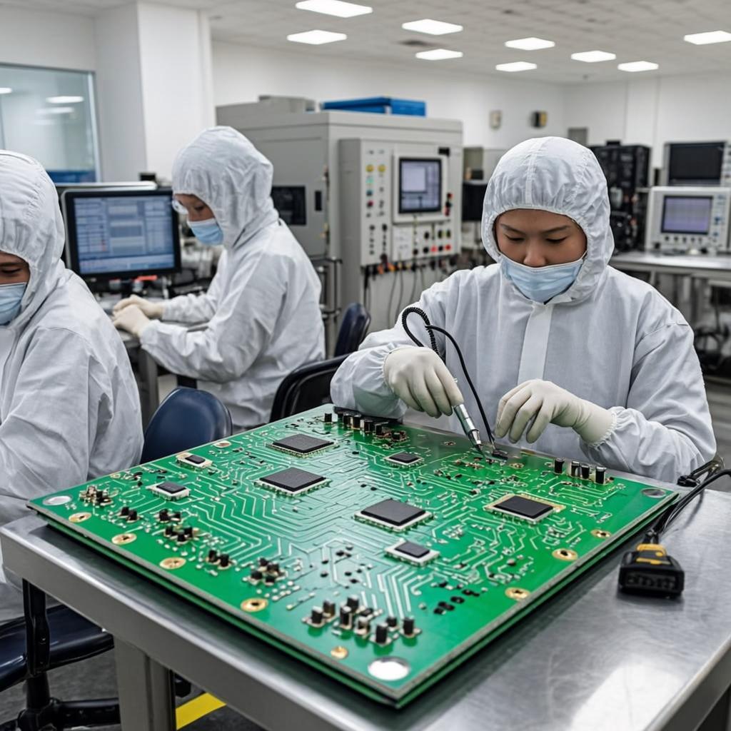
At this stage, the PCB is subjected to rigorous testing and inspection to ensure that all components are correctly placed and soldered. Automated optical inspection (AOI) and X-ray inspection are commonly used methods to detect issues such as soldering defects, misalignments, and missing components. Additionally, functional testing is carried out to check the overall performance of the PCB.
Once the PCB passes inspection and testing, the final assembly process begins. Additional components or enclosures may be added to the PCB, depending on the final product requirements. The fully assembled product is then ready for shipment to customers or for integration into a larger system.
Wintech is a leading provider of turnkey PCB assembly services, specializing in high-mix, low-to-mid volume electronics manufacturing. With a proven track record of delivering customized and state-of-the-art solutions, Wintech is well-equipped to handle complex PCB assembly needs. They offer:
Investing in high-quality PCB assembly offers numerous benefits to electronics manufacturers, including:
The PCB assembly manufacturing process is a multi-step procedure that ensures the creation of reliable and functional electronic products. Companies like Wintech provide end-to-end PCB assembly solutions, offering high-quality services tailored to meet customer specifications. Whether for high-mix, low-volume production or large-scale manufacturing, understanding the PCB assembly flow is crucial for any business involved in electronics production.