A PCB assembly line is a highly coordinated manufacturing system designed to turn bare printed circuit boards (PCBs) into fully functional electronic assemblies. Each stage in the line adds components, applies solder, and ensures electrical connections are precise and reliable. In simple terms, it’s the process that transforms a blank board into the “brain” of an electronic device.
It’s important to distinguish PCB fabrication from PCB assembly.
PCB fabrication is the process of creating the physical board itself — etching copper layers, drilling vias, and laminating materials to form the substrate.
PCB assembly, on the other hand, involves mounting and soldering electronic components onto that fabricated board to make it operational.
In the electronics supply chain, the assembly line plays a crucial role in bridging design and delivery. Prototypes are first produced to validate functionality, and once approved, the same assembly line can be scaled for mass production. This ensures consistent quality, faster time-to-market, and cost efficiency for products ranging from consumer gadgets to industrial control systems.
A modern PCB assembly line is built around precision automation and quality control. The main equipment typically includes:
Example: In a mid-volume manufacturing plant, a typical SMT (Surface Mount Technology) assembly line might begin with a solder paste printer, followed by two high-speed pick-and-place machines, a reflow oven, and an AOI station at the end. This streamlined setup allows continuous operation — placing thousands of components per hour while maintaining strict quality control.
In essence, every element of a PCB assembly line is designed for efficiency, accuracy, and repeatability, ensuring that each circuit board leaving the line meets the exact specifications required for modern electronic products.
The PCB assembly process is a carefully coordinated sequence of steps that ensures every electronic component is accurately mounted and soldered onto the printed circuit board. Each stage builds upon the previous one, combining precision, automation, and quality control to create reliable electronic assemblies.
The first step in the PCB assembly line is solder paste printing. Its purpose is to apply a thin layer of solder paste onto the designated pads of the PCB, where components will later be mounted. The paste, a mixture of tiny solder particles and flux, acts as both an adhesive and an electrical connector once heated.
The key equipment for this process includes a solder paste printer and a stainless-steel stencil. The printer aligns the stencil over the board and spreads the paste evenly across the surface, ensuring each pad receives the right amount.
Common issues include misalignment, which can lead to misplaced components, and insufficient or excess solder paste, which may cause weak joints or solder bridges.
Example: Modern assembly lines use automated stencil alignment systems with optical sensors to correct positioning in real time, improving yield and consistency.
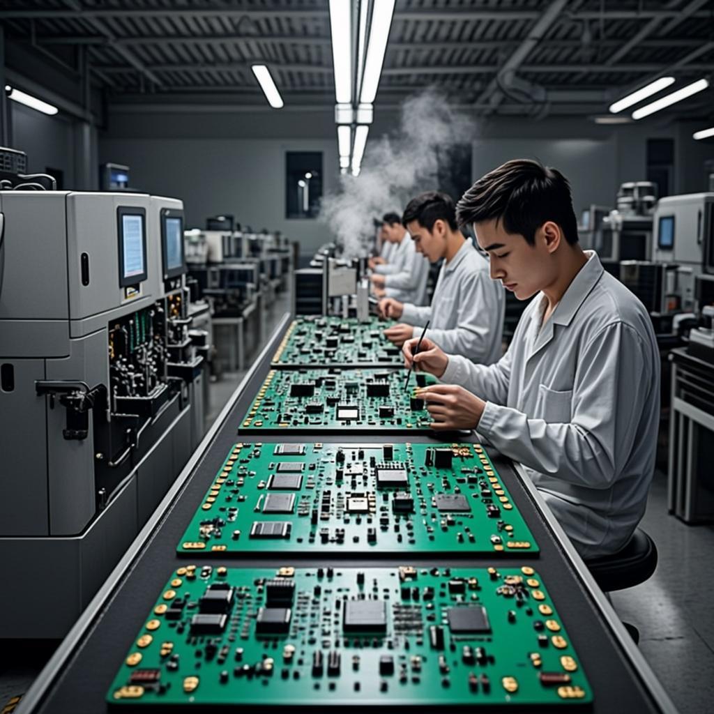
Next comes component placement, where electronic parts are positioned on the PCB. This step is typically performed using SMT pick-and-place machines, which use robotic arms and vision systems to pick components from reels and place them precisely on the solder-pasted pads.
For prototypes or small batches, components may be placed manually under a microscope. However, for volume production, automated machines dominate — capable of placing thousands of parts per hour with sub-millimeter accuracy.
Example: A high-speed pick-and-place system can mount tiny 0402 resistors and complex ICs in seconds, ensuring accuracy even at high throughput.
Once all components are placed, the board moves to the reflow soldering stage. Here, controlled heat is applied to melt the solder paste and create strong, permanent electrical joints.
The process follows four distinct temperature stages:
Example: In convection reflow ovens, hot air circulates to heat the PCB uniformly, while vapor-phase ovens use a controlled vapor medium for even better thermal transfer in sensitive assemblies.
After soldering, every PCB undergoes inspection and quality control to identify defects before they progress downstream. The most common methods include:
Early detection of issues such as solder bridges, cold joints, or missing components prevents costly rework later in production.
Example: AOI systems use AI-driven algorithms to automatically flag deviations from reference images, reducing false positives and increasing inspection speed.
While SMT dominates modern electronics, some designs still require Through-Hole Technology (THT) — where components with wire leads are inserted into drilled holes in the PCB. This technique is often used for connectors, large capacitors, or high-power parts needing extra mechanical strength.
Insertion can be manual for small batches or automated using insertion machines in high-volume production. After insertion, components are soldered using wave soldering (where molten solder flows under the board) or selective soldering (targeted application for specific areas).
Before shipment, each assembled PCB is tested to verify electrical performance. The two most common methods are:
Example: Functional test fixtures connect to the PCB through test points, measuring voltage, current, and signal behavior to ensure the product meets design specifications.
The final stage involves post-testing procedures that prepare the PCB for delivery. This includes cleaning (to remove flux residues), conformal coating (for moisture or dust protection), labeling, and packaging for shipment.
Manufacturers also maintain traceability systems using barcodes or lot tracking to record production data for each batch. This ensures accountability, supports quality audits, and simplifies after-sales service.
Each of these steps — from solder paste printing to final packaging — forms part of a continuous, data-driven workflow that defines a modern PCB assembly line. Together, they ensure every circuit board meets the performance, reliability, and consistency demanded in today’s electronics manufacturing industry.
A PCB assembly line relies on a series of precision-driven machines that work together to ensure speed, accuracy, and consistency. Each piece of equipment plays a unique role — from applying solder paste to inspecting finished boards — making the entire process efficient and reliable.
The solder paste printer is the first and one of the most critical machines in the PCB assembly process. It applies a thin layer of solder paste onto the copper pads of the PCB through a metal stencil, creating the foundation for all subsequent steps.
High precision is essential — even a slight misalignment can cause solder bridging or open circuits later in production. Most modern printers use automatic vision alignment systems to detect fiducial marks on the PCB and perfectly align the stencil before printing.
Regular maintenance, such as cleaning the stencil and calibrating the squeegee pressure, is vital to maintain consistent print quality and prevent defects.
Example: In a high-volume SMT line, an automatic printer with closed-loop feedback control can adjust paste pressure and alignment in real time, improving yield and reducing operator intervention.
The pick-and-place machine is the workhorse of the PCB assembly line. It automatically picks tiny electronic components from reels or trays and places them onto the solder-pasted PCB pads with extreme speed and precision.
Performance is often measured in CPH (components per hour) — high-speed models can place over 100,000 components per hour, depending on board complexity.
There are two main types of pick-and-place systems:
A well-balanced SMT line often combines both types to maximize throughput and placement accuracy.
Once components are placed, the board enters the reflow oven, where controlled heat melts the solder paste and creates permanent electrical and mechanical joints. The process is governed by a temperature profile — a time-based curve that defines the ideal heating and cooling cycle for a specific solder type and component layout.
A standard reflow profile includes four stages: preheat, soak, reflow, and cooling. Each stage must be carefully calibrated to prevent solder defects such as voids or cold joints.
Different oven technologies offer distinct advantages:
Optimization often involves adjusting belt speed and zone temperatures based on board size and component mix to ensure consistent solder quality.
Automated Optical Inspection (AOI) and X-Ray inspection systems are the quality guardians of the PCB assembly line. Their main role is to detect defects early, ensuring that only flawless boards proceed to the next stage.
AOI Systems use high-resolution cameras and image recognition software to identify missing, misaligned, or incorrect components, as well as soldering issues.
X-Ray Systems are used for hidden solder joints, such as those under BGAs or QFNs, where optical inspection isn’t possible.
Modern systems increasingly leverage AI-driven inspection algorithms that can learn from previous defect data, improving accuracy over time while reducing false rejections.
Example: In a smart manufacturing environment, AI-enhanced AOI systems automatically flag patterns of recurring defects, enabling real-time process adjustments and predictive maintenance — a key feature of Industry 4.0-ready assembly lines.
In essence, the efficiency and quality of a PCB assembly line depend heavily on how these machines operate together. A precisely tuned combination of printing, placement, soldering, and inspection equipment ensures high yield, minimal downtime, and consistent product performance across every production run.
In electronics manufacturing, SMT (Surface Mount Technology) and THT (Through-Hole Technology) represent two distinct methods of assembling components onto a printed circuit board. Each has unique advantages, applications, and equipment requirements, and understanding the difference helps engineers and procurement teams choose the right process for their products.
Surface Mount Technology (SMT) is the most widely used assembly method.