FR-4 multilayer PCB manufacturing from standard to high-Tg with HDI microvias, controlled impedance ±5% (plus/minus five percent), low-loss stackups for 10–25 Gbps, and 12-hour express builds. Get a fast quote today.
Material strategy that matches thermal and signal targets
Standard FR-4 (Tg 130–140°C) fits consumer and general embedded designs with moderate heat. Mid-Tg (150–160°C) adds margin for denser multilayers and localized heating. High-Tg (170–180°C) supports multiple lead-free reflow cycles up to 260°C (two hundred sixty degrees Celsius) and higher ambient operation in automotive or industrial environments. For signal layers above 10–12 Gbps, low-loss FR-4 (Df 0.009–0.012) reduces insertion loss by roughly 0.1–0.2 dB per inch (geometry dependent). Our multilayer PCB and HDI PCB capabilities enable hybrid stackups to balance cost with performance.
Inadequate material selection or over-lamination may trigger glass-fiber recession, resin starvation, or delamination during multiple reflow cycles, especially when operating near Tg or under high-current loading. Poor dielectric control can also distort impedance targets above 10 Gbps (ten gigabits per second).
We validate each FR-4 material with IPC-4101 and IPC-6012 conformance testing, monitoring Z-axis expansion and Td (>300°C — greater than three hundred degrees Celsius). Controlled prepreg flow and symmetric stackups ensure planar lamination and stable impedance (±5% — plus/minus five percent). For high-speed or high-temperature environments, our High-Tg PCB and high-frequency material solutions provide additional reliability margin.
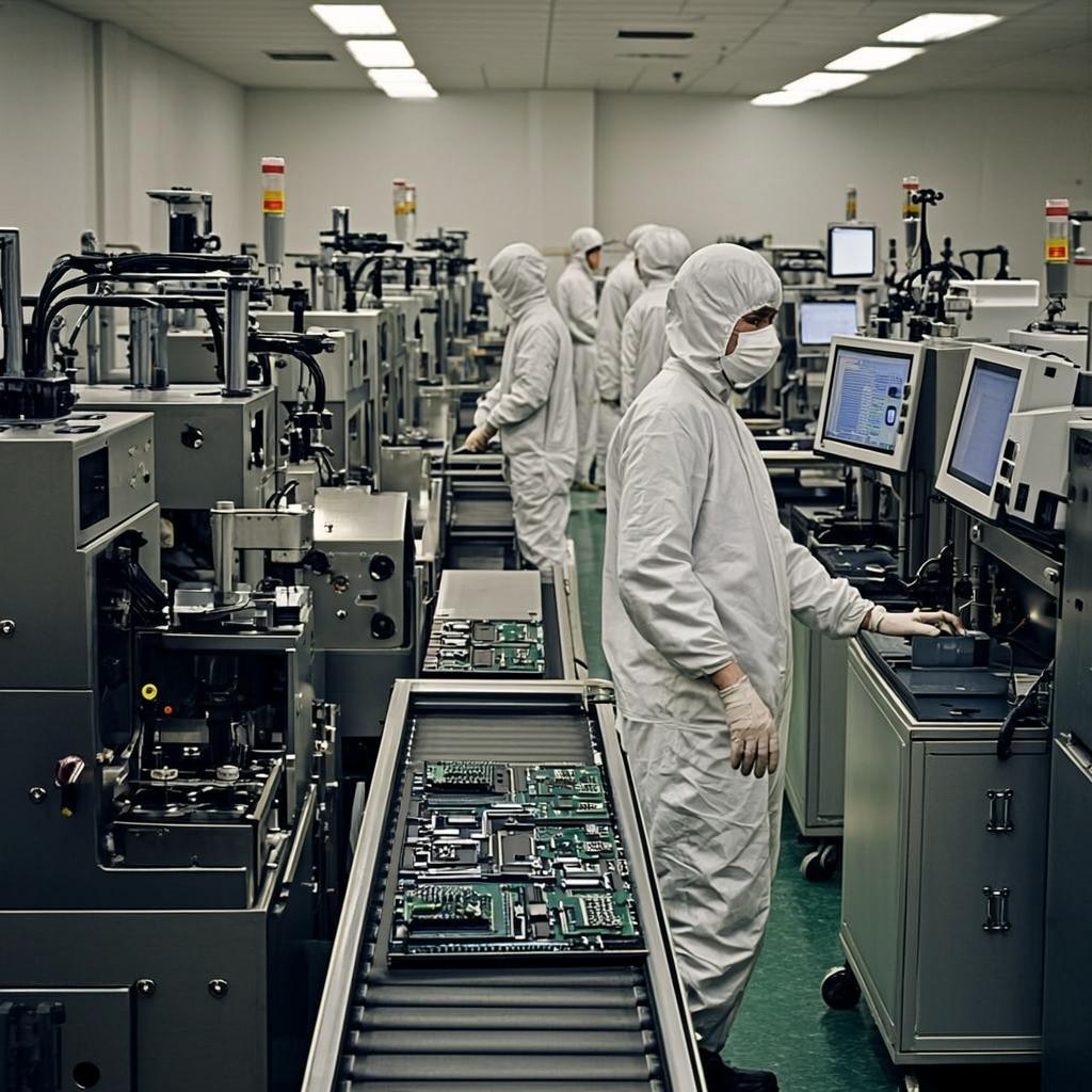
Process control with statistical monitoring and 100% testing
Laser direct imaging (LDI) delivers registration accuracy within ±12.5 µm (plus/minus twelve point five micrometers) across sequential lamination. Mechanical drilling supports 0.20 mm (eight mil) holes; laser microvias reach 0.075 mm (three mil). Pulse-reverse plating keeps via copper thickness variation within ±10% (plus/minus ten percent) for impedance consistency. RF and high-speed builds use TDR coupons to confirm impedance within ±5% (plus/minus five percent); for methodology see our impedance control guide.
HDI flows include plasma desmear, filled microvias and planarized build-ups (1+n+1 to 3+n+3) supporting 0.3 mm BGA pitch. Coverage extends with AOI, X-ray and 100% electrical test; acceptance criteria align to IPC-A-600/IPC-6012—see notes in IPC-6012 performance.
Compliant with IPC-A-600 Class 2/3 and IPC-6012
Whether you need simple prototypes or complex production runs, our advanced manufacturing capabilities ensure excellent quality and reliability. Get your quote within 30 minutes.
Choose standard FR-4 for general purpose; move to low-loss when insertion loss budgets tighten or when channels exceed 10–12 Gbps. Hybrid stackups can place low-loss material under high-speed pairs while keeping FR-4 cores elsewhere. For modeling tips and tolerances, see impedance control and high-frequency materials. If dense routing or BGA escape drives feature sizes below 75 µm (seventy-five micrometers), consider HDI PCB.
Incoming laminate checks follow IPC-TM-650; DSC Tg checks target ±2°C (plus/minus two degrees Celsius) accuracy. Microsections confirm via plating ≥20 µm Class 2 / ≥25 µm Class 3 (greater than or equal to twenty / twenty-five micrometers) with controlled etchback and void limits <0.5% (less than zero point five percent). Time-domain reflectometry (TDR) verifies impedance within ±5% using stackup-matched coupons. For acceptance details, see our IPC-6012 notes.
Automotive ECUs benefit from high-Tg FR-4 for under-hood thermal margin; industrial control demands thicker copper planes and robust dielectric spacing; telecom/datacom line cards combine impedance control with low-loss layers to maintain eye openings. For assembly readiness and faster ramps from proto to pilot, see our SMT assembly services.
Each FR-4 program includes DFM/DFT reviews, coupon strategy and lamination windows tuned to copper balance and resin content.
Registration, plating thickness and dielectric spacing are monitored with SPC; Cpk targets (e.g., Cpk ≥ 1.33 — greater than or equal to one point three three) are enforced on critical parameters.
Workmanship aligns to IPC-A-600/IPC-6012 with 100% AOI and electrical testing; audits are supported under ISO 9001 and IATF 16949/ISO 13485 when applicable.
MES links supplier lots, panel serialization and TDR results for traceability and rapid root-cause analysis.
Use high-Tg (170–180°C) for multiple lead-free reflows, under-hood or industrial environments; choose low-loss (Df 0.009–0.012) when channels exceed 10–12 Gbps or insertion loss is margin-limiting.
We control dielectric thickness and copper geometry, include matched coupons and verify with TDR; production data is correlated to field solver models to maintain ±5% (plus/minus five percent).
Gerber/ODB++, stackup intent, target impedance (single-ended/differential), material preferences (standard, high-Tg, low-loss), test requirements and volumes.
Yes. We provide laser microvias down to 0.075 mm (three mil) with filled/stacked options and sequential lamination (1+n+1 to 3+n+3) for 0.3 mm BGA pitch.
From simple prototypes to complex production runs, our world-class factory delivers superior quality, fast turnaround and competitive pricing. Join thousands of satisfied customers who trust us with their PCB manufacturing needs.