A PCB substrate is a dielectric layer that acts as an insulator between two copper layers in a stack-up. Based on its properties, it can alter the effects of signal attenuation, crosstalk, and electromagnetic radiation, which directly impacts the signal integrity. For instance, a low Dk PCB material such as Rogers 4350B will exhibit lower losses even at high frequencies when compared to standard FR4.
If you’re working on aerospace or automotive designs, the board needs to sustain high temperatures, humidity, and stress while operating in a harsh environment. Hence, it needs to be mechanically robust and chemically stable. In short, understanding the characteristics of the dielectric is crucial for fabricating a quality printed circuit board.
In this article, we will discuss the electrical, mechanical, thermal, and chemical properties of a substrate which will help you choose the right material for your design.
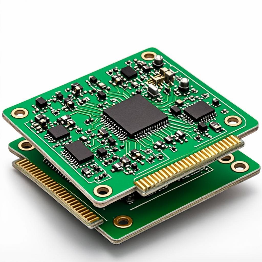
Dielectric material provides insulation between conducting layers (shown as copper foil) in a PCB.
Glass transition temperature, or Tg, is the temperature range in which a PCB substrate transitions from a glassy, rigid state to a softened, deformable state as polymer chains become more mobile. When the material cools back down, its properties return to their original states. Tg is expressed in units of degrees Celsius (ºC).
Decomposition temperature, or Td, is the temperature at which a PCB material chemically decomposes (the material loses at least 5% of mass). Like Tg, Td is expressed in units of degrees Celsius (ºC).
A substrate’s Td is an important ceiling when assembling PCBs, because when a material reaches or surpasses its Td, changes to its properties are not reversible. Contrast this to Tg, glass transition temperature, where properties will return to their original states once the material cools below the Tg range.
Choose a material where you can work in a temperature range that’s higher than Tg but well below Td. Most solder temperatures during PCB assembly are in the 200 ºC to 250 ºC range, so make sure Td is higher than this (luckily, most materials have a Td greater than 320 ºC).
The coefficient of thermal expansion, or CTE, is the rate of expansion of a PCB material as it heats up. CTE is expressed in parts per million (ppm) expanded for every degree Celsius that it is heated.
As a material’s temperature rises past Tg, the CTE will rise as well.
The CTE of a PCB substrate is usually much higher than copper, which can cause interconnection issues as a PCB is heated.
CTE along the X and Y axes are generally low – around 10 to 20 ppm per degree Celsius. This is usually thanks to the woven glass that constrains the material in the X and Y directions, and the CTE doesn’t change much even as the material’s temperature increases above Tg.
So the material must expand in the Z direction. The CTE along the Z axis should be as low as possible; aim for less than 70 ppm per degree Celsius, and this will increase as a material surpasses Tg.
A material’s expansion is measured by the coefficient of thermal expansion (CTE). This image shows CTE in the Z direction.
The point at which the displacement is maximum on the CTE curve is referred to as glass transition temperature (Tg). If the temperature is higher than the Tg, the substrate softens and doesn’t expand any further.
Thermal conductivity, or k, is the property of a material to conduct heat; low thermal conductivity means low heat transfer while high conductivity means high heat transfer. The measure of the rate of heat transfer is expressed in watts per meter per degree Celsius (W/M -ºC).
Most PCB substrates have a thermal conductivity in the range of 0.3 to 0.6 W/M-ºC, which is quite low compared to copper, whose k is 386 W/M-ºC. Therefore, more heat will be carried away quickly by copper plane layers in a PCB than by the dielectric material.
Considering the dielectric constant of a material is important for signal integrity and impedance considerations, which are critical factors for high-frequency electrical performance. The Er for most PCB materials is in the range of 2.5 to 4.5.
The dielectric constant varies with frequency and generally decreases as frequency increases; some materials have less of a change in relative permittivity than others. Substrates suitable for high-frequency applications are those whose dielectric constant remains relatively the same over a wide frequency range–from a few 100MHz to several GHz.
When a signal propagates through a substrate, its dielectric constant alters the signal behavior. This is because the EM wave emitted is not confined to the trace and passes through the substrate. This can cause severe signal integrity issues. This effect will be even more significant at high frequencies.
The speed of the propagating EM wave is inversely proportional to the dielectric constant. Hence, a low Dk PCB material will have the following advantages:
Even with all the advantages, the dispersion in the low Dk PCB material still exists, which can distort the digital signals. They are also more expensive than FR4. They may also need higher temperatures and pressure during the board fabrication process, which can drive the cost even higher. A few examples of high-speed materials include Rogers 4350B, RT Duroid 5880, and Isola-I speed.
Even though we associate power integrity with constant voltage input, the dielectric constant also affects the stability of the input power. If you place a high Dk material between the power and ground layers, the interplanar capacitance will become significant.
The planes themselves act as a large decoupling capacitor which helps to maintain a constant input voltage. It also lowers the PDN impedance. However, a higher Dk will result in increased dielectric loss, crosstalk, and EMI issues. In order to balance power and signal integrity, it is advised to opt for a hybrid stack-up of high and low Dk PCB materials.
A higher dielectric constant substrate can be used for separating the power and ground layer whereas the lower Dk substrate supports the signal layer with less loss. Manufacturing hybrid stack-ups depends on manufacturer capabilities as they have to consider the difference in CTE of the materials used.
A material’s loss tangent gives a measure of the power lost due to the material. The lower a material’s loss tangent, the less power is lost. The Tan δ of most PCB materials ranges from 0.02 for most commonly used materials to 0.001 for very low-loss high-end materials. It also varies with frequency, increasing as frequency increases. Read the difference between microstrip and stripline in PCBs.
Loss tangent isn’t usually a critical consideration for digital circuitry, except at very high frequencies above 1 GHz. However, it is a very important parameter for analog signals, as it determines the degree of signal attenuation and thus affects the signal-to-noise ratio at various points along signal traces.
The dielectric constant significantly impacts the controlled impedance and the width of the conductor. If the Dk is higher, then the trace width required will be lower to achieve the target impedance.
Volume resistivity, or electrical resistivity (ρ), is one of the measures of the electrical or insulation resistance of a PCB material. The higher a material’s resistivity, the less readily it allows the movement of electric charge and vice versa. Resistivity is expressed in ohm-meters (Ω-m) or ohm-centimeters (Ω-cm)
As dielectric insulators, circuit board substrates are required to have very high values of resistivity, in the order of 10⁶ – 10¹⁰ Megaohm-centimeters. Resistivity is somewhat affected by moisture and temperature.
Surface resistivity (ρS) is the measure of the electrical or insulation resistance of the surface of a circuit board substrate. Like volume resistivity, PCB materials are required to have very high values of surface resistivity, in the order of 10⁶ — 10¹⁰ Megaohms per square. It is also somewhat affected by both moisture and temperature.
Electrical strength measures a PCB substrate’s ability to resist electrical breakdown in the PCB’s Z direction (perpendicular to the PCB’s plane). It is expressed in Volts/mil. Typical electrical strength values for PCB dielectrics are in the range of 800 V/mil to 1500 V/mil.
Electrical strength is determined by subjecting the PCB material to short high-voltage pulses at standard AC power frequencies.
UL94, or the Standard for Safety of Flammability of Plastic Materials for Parts in Devices and Appliances testing, is a plastics flammability standard that classifies plastics from lowest (least flame-retardant) to highest (most flame-retardant).
The standards are defined by Underwriters Laboratories (UL). Most PCB substrates adhere to UL94 V-0; here are its requirements
Moisture absorption is the ability of a board substrate to resist water absorption when immersed in water. It is given by a percentage increase in the weight of a PCB material due to water absorption under controlled conditions as per standard test methods. Most substrates have moisture absorption values in the range of 0.01% to 0.20%.
Moisture absorption affects the thermal and electrical properties of the substrate, as well as the ability of the material to resist conductive anode filament (CAF) formation when a PCB circuit is powered.
Methylene chloride resistance is a measure of a material’s chemical resistance; specifically, the ability of a PCB material to resist methylene chloride absorption.
Just like moisture absorption, it is expressed by a percentage increase in the weight of a PCB material due to exposure to or soaking in methylene chloride under controlled conditions. Most PCB materials have methylene chloride resistance values in the range of 0.01% to 0.20%.
Michael J. Gay,Director, High-Performance Products, Isola Group, stated that “Moisture is one of the sources of Dk variation in PCB materials. There are other possible sources that could potentially result in some minor variation, but moisture uptake over time is a fairly large potential factor.” The below chart shows the moisture uptake in a 24-hour DI water soak at various temperatures for Tachyon 100G material.
Dielectric constant Vs. temperature for a low Dk PCB material Tachyon 100 G. Image credit: Isola Group
Michael further explained, “As you can see, the Dk is about 0.02 higher after the material becomes saturated at 23 °C or room temperature. It is not a huge difference, but it might make you think of changing the line width requirement to center the impedance. Moisture uptake would happen to the clad laminate over many weeks or to the etched laminate over several hours. Uptake is dependent on the length of the path for the material to reach equilibrium. For example, a single etched signal layer core sitting in AOI for a few hours would pick up the maximum moisture content at RT (relative temperature). These areas are usually about 60% RH (relative humidity) and so moisture is readily available.”
In an actual PCB design, the moisture may not stay in the areas near hot components and be driven out of the board when temperatures reach 80-90 °C near hot chips.