Helen Frankenthaler PCB Circuit Board R&D Center

multilayer pcb hs code

High-Quality Multilayer PCB Manufacturing - KKPCB

Multilayer PCB Manufacturing Multilayer PCB with Blind/Buried Via & Mixed Material

KKPCB specializes in the manufacturing of high-quality multilayer printed circuit boards designed for advanced and high-reliability electronic applications. With state-of-the-art equipment and precise process control, we are capable of producing complex multilayer PCBs featuring blind and buried vias, mixed materials, and fine traces. Our experienced engineering team provides full DFM support to ensure manufacturing accuracy, signal integrity, and cost efficiency. Trusted by customers worldwide, KKPCB continues to deliver multilayer PCB solutions that combine innovation, performance, and reliability.

What is multilayer PCB?

Multilayer PCB board refers to a PCB that has more than three conductive pattern layers and is laminated with insulating materials between them. With the development of electronic technology to high-speed, multi-function, large capacity, and portable low-consumption direction, the application of multi-layer PCB is more and more widely, and its layer number and density are also higher and higher, and the corresponding structure is also increasingly complex. The production of multilayer PCB has become the most important part of the whole PCB industry. At present, the average number of layers of KKPCB has reached 8-20 layers, can up to 64 layers, which has reached a high level in terms of inner layer manufacturing ability and laminating ability. The emergence of multi-layer board technology is a major development of the PCB industry, which makes the whole PCB technology advance by leaps and bounds.

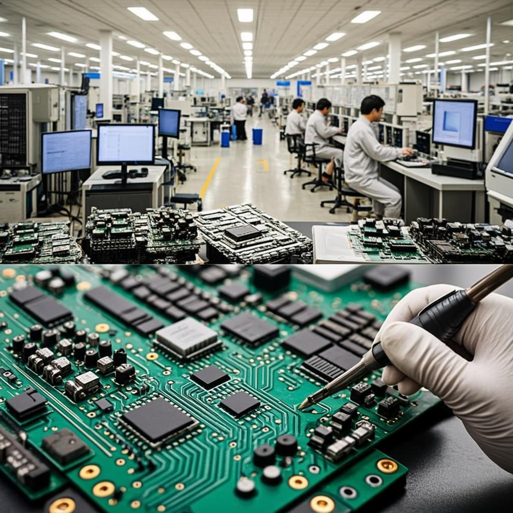
KKPCB is very good at multilayer PCB fabrication and prototyping. The manufacturing process of ordinary multilayer PCB is mainly based on lamination technology. Multi-layer lamination is an important process in PCB manufacturing. KKPCB has been producing multilayer PCBs for over 20 years. Over the years, we have seen all types of multilayer constructions from various industries, answered all types of multilayer questions, and solved all types of problems with multilayer PCBs.

Multilayer PCB Lamination

  • The thickness of the core board should be selected according to the total thickness requirements of the multilayer board. The thickness of the core board should be consistent and the deviation is small.
  • There should be a certain distance between the overall dimension of the core board and the effects unit, that is, the distance from the effective unit to the edge of the board should be on the premise of not wasting materials try to keep more space.
  • Design of positioning hole. In order to reduce the deviation between layers, attention should be paid to the design of positioning holes in multi-layer boards: 4-layer multilayer only needs to be designed more than 3 positioning holes can be used for drilling. For multi-layer boards with more than 6 layers, in addition to designing positioning holes for drilling, it is also necessary to design more than 5 overlapping positioning rivet holes and more than 5 positioning holes for the tool plate for rivets.
  • The inner core board shall be free from the open, short, open circuit, oxidation, clean board surface, and no residual film.
  • Meet the requirements of PCB users, select the appropriate PP and copper foil configuration. For 4-ply laminates, 7628, 3313 or 7628 + 1080, 7628 + 2116 can be used etc. 1080 or 2116 is the main choice of PP for multilayer boards with more than 6 layers, and 7628 is mainly used to increase the thickness of the dielectric layer. At the same time, PP requires symmetrical placement to ensure mirror effect and prevent plate bending.
  • Inner core board pretreatment process. The treatment process of the inner layer core board includes the black oxidation process and browning treatment process. The oxidation treatment process is to form a black oxide film on the inner copper foil, the thickness of the black oxide film is 0.25-4.50mg/cm2. The browning process (horizontal browning) is to form an organic film on the inner copper foil.

The functions of the inner laminate treatment process are as follows:

  • Increasing the surface ratio of inner copper foil and resin can enhance the adhesion between them.
  • The effective wettability of the melt resin to copper foil is increased so that the flowing resin has sufficient ability to penetrate into the oxide film and show a strong grip after curing.
  • It can prevent the decomposition of dicyandiamide in liquid resin at high temperatures and influence on the copper surface.
  • It can improve the acid resistance and prevent the PINK ring in the wet process.

The organic matching of lamination parameters, the control of multi-layer board lamination parameters mainly refers to the organic matching of lamination “temperature, pressure, and time”. How to determine the lamination temperature, pressure, and time software parameters is the key technology for multilayer laminate processing.

Materials for making multilayer PCB

1. Copper Foil

Function: Forms the conductive patterns on the PCB.

Description: Copper foil is the essential material for the PCB’s conductive layers, providing the electrical pathways necessary for signal transmission and overall board performance.

2. Core Board

Function: Serves as the structural framework of the PCB.

Description: A double-sided copper-clad laminate that acts as the backbone of the circuit board. Core boards provide mechanical stability and serve as the foundation for double-sided or multilayer PCB production.

3. Prepreg

Function: Acts as both adhesive and insulator between core boards in multilayer PCBs.

Description: Prepreg is an indispensable material in multilayer PCB manufacturing. It bonds core boards together while providing electrical insulation. During lamination, prepreg ensures strong interlayer adhesion, preventing short circuits and maintaining structural integrity.

Material NameMaterial TypeBase Thickness (μm)
FR47628193
1506150
2116122
331399
108074
10660
Difference Between Single-Layer and Multilayer PCBs

Compared with single-layer or double-layer PCBs, multilayer PCBs offer significantly improved electromagnetic compatibility (EMC) and enhanced electrical performance.

For example, in a four-layer PCB, the inner layers are often designated as a power plane and a ground plane, which provides the following benefits:

  • Reduced Inductance: The inductance of power and ground traces is greatly reduced, lowering noise voltage.
  • High-Frequency Decoupling: The power and ground planes form a large distributed capacitor, providing excellent high-frequency decoupling for the power supply and reducing power line noise.
  • Minimized Signal Loops: Independent power and ground planes help minimize the loop area for all signal paths, improving signal integrity.
  • Industry Trend Toward Miniaturization: Modern PCBs are trending toward smaller sizes, thinner layers, smaller vias, higher layer counts, and finer trace widths and spacing—making multilayer designs essential.
  • Support for Advanced Electronics: Many high-precision and high-tech electronic devices require multilayer PCBs to achieve their functions. Standard double-sided boards cannot meet these advanced requirements.

Conclusion: Multilayer PCBs are indispensable for modern electronics, providing superior noise control, signal integrity, and support for compact, high-density circuit designs.

Types of Multilayer PCBs

1. Classification by Application
  • Consumer Electronics PCBs: Used in TVs, electronic toys, smartphones, and other consumer devices.
  • Industrial PCBs: Used in computers, instrumentation, automation systems, and other industrial equipment.
  • Military & Aerospace PCBs: Designed for high-reliability applications in defense and aerospace, often meeting strict environmental and performance standards.
2. Classification by Flexibility / Hardness
  • Rigid PCBs: Solid, inflexible boards for traditional electronic devices.
  • Flexible PCBs (Flex): Can bend or fold to fit compact spaces or dynamic applications.
  • Rigid-Flex PCBs: Combination of rigid and flexible sections, ideal for high-density, complex assemblies.
3. Classification by Via / Hole Technology
  • Buried Via PCBs: Vias that connect inner layers without reaching the outer layers.
  • Blind Via PCBs: Vias that connect outer layers to inner layers without going through the entire board.
  • Blind-Buried / HDI PCBs: High-Density Interconnect PCBs combining blind and buried vias for miniaturized, high-performance circuits.
  • Through-Hole PCBs: Vias that pass through all layers of the board, commonly used for mounting components.
4. Classification by Substrate Material
  • FR4 (Glass Cloth) PCBs: Standard rigid boards based on glass-epoxy material.
  • Ceramic Substrate PCBs: Used for high-frequency, high-temperature, or high-power applications.
  • Metal-Core PCBs (MCPCBs): Offer excellent heat dissipation for LED and power applications.

Application of Multilayer PCB

As mentioned above, multilayer PCB can be used in civil, industrial, and military fields. Multilayer PCB can be used for any purpose.

For many industries, multilayer PCB has become the first choice for various applications. This preference is largely due to the continuous promotion of mobility and functionality by all technologies. Multilayer PCB is a reasonable step in this process, which can reduce the size and realize more functions. As a result, they have become quite common, including:

  • Consumer electronics: consumer electronics is a broad term, such as smartphones and microwave ovens. Each of these consumer electronics products contains PCB, but more and more of them use multilayer PCB instead of standard single-layer PCB, which is used to increase function and reduce size.
  • Computer electronics: everything from the server to the motherboard uses multilayer PCBs, mainly because of their space-saving and high functionality. For these applications, performance is one of the most basic characteristics of PCB.
  • Telecommunications: telecommunications equipment typically uses multilayer PCBs in a variety of general applications, such as signal transmission, GPS, and satellite applications. The main reason is its durability and functionality.
  • Industrial: Multilayer PCB has become popular in several industrial applications, the most notable of which is industrial control. From industrial computers to control systems, multilayer PCBs are used to run machines throughout manufacturing and industrial applications, contributing to their durability and small size.
  • Medical devices: electronic products are becoming an increasingly important part of the healthcare industry, playing a role in every corner of the industry, from treatment to diagnosis. Compared with single-layer substitutes, multilayer PCB is particularly popular in the medical industry because of its small size, lightweight and powerful functions. These advantages make multilayer PCB used in modern X-ray equipment, cardiac monitor, CAT scanning equipment, and medical test equipment.
  • Military and national defense: multilayer PCBs are favored in terms of durability, functionality, and low weight, and are very useful in high-speed circuits, which are getting more and more attention in military applications. As the defense industry moves towards highly compact engineering, they are also favored, as smaller multi-layer PCBs leave more space for other components to perform their existing functions.
  • Automobile: in the modern automobile, the automobile is more and more dependent on electronic components, especially with the rise of an electric vehicles. From GPS and onboard computers to headlight switches and engine sensors controlled by electronic devices, using the right type of components is becoming increasingly important in vehicle design. Multilayer PCB has high function and relative heat resistance, so it is very suitable for the interior environment of automobiles.
  • Aerospace: like cars, jets, and KKPCB, they rely heavily on modern electronics, all of which have to be very precise. From the computer used on the ground to the computer used in the cockpit, the application of aerospace PCB must be reliable. In this case, multilayer PCB is the ideal solution, with enough protection layer to keep heat and external stress from damaging the connection, and the ability to be made of flexible materials. Their higher quality and functionality also contribute to this utility in the aerospace industry, as aerospace companies prefer to use the best materials to ensure the safety of personnel and equipment.
  • There are more! Multilayer PCB is used in a variety of other industries, including the science and research industry, even household appliances and safety. All devices, from alarm systems and optical fiber sensors to atomic accelerators and weather analysis equipment, use multilayer PCBs, making full use of the space and weight saved by this PCB format.

KKPCB is widely known as a professional PCB supplier in the electronic manufacturing industry. We have years of experience in the multilayer PCB, HDI PCB