Helen Frankenthaler PCB Circuit Board R&D Center

multilayer pcb maker

What is the cost of manufacturing multilayer PCB?

What is the cost of manufacturing multilayer PCB?

Table of Contents

  • Multidimensional Analysis of PCB Cost Structure
  • Quantitative Analysis of Layer Count Impact on Cost
  • Cost Premium Analysis of Advanced Processes
  • Engineering Practices for Cost Optimization
  • Industry Cost Trend Forecast
  • Topfast’s Advantages in Multilayer Board Manufacturing

Multidimensional Analysis of PCB Cost Structure

As the core carrier of electronic systems, the manufacturing cost of PCBs is influenced by a variety of factors, including materials, processes, design complexity, and quantity. According to the IPC-6012 standard, the cost structure of modern PCBs can be broken down into the following key dimensions:

The specific price is subject to actual communication.

  • Substrate Cost (25-40% of total cost):
    • Standard FR-4 epoxy glass cloth substrate: ¥50-150/m²
    • High-frequency materials (e.g., Rogers RO4003C): ¥800-2000/m²
    • High TG materials (TG170+): 30-50% higher than standard FR-4
    • Aluminum substrate (IMS): ¥300-800/m²
  • Copper Foil Cost (15-25% of total cost):
    • Standard 1oz (35μm) electrolytic copper foil: Base price
    • 2oz copper foil: 35-40% cost increase
    • 3oz+ thick copper: Exponential cost growth
  • Process Cost (30-45% of total cost):
    • Standard through-hole board process: Baseline cost
    • Blind/buried via process: 20-30% cost increase
    • HDI (High Density Interconnect) process: 50-100% cost increase
    • Impedance control requirements: 15-25% additional cost

Looking for cost-effective PCB solutions? Get an instant quote tailored to your project needs!

Quantitative Analysis of Layer Count Impact on Cost

The relationship between PCB layers and cost shows nonlinear growth, determined by the following engineering factors:

LayersCost FactorKey Technical Challenges
1-21.0xBasic process, yield >95%
41.8-2.2xLamination alignment accuracy ±50μm
62.5-3.0xInner layer AOI inspection required
83.5-4.5xInterlayer dielectric uniformity control
10+5.0x+Requires a segmented lamination process

Notably, 4-6 layer boards offer the best cost-performance ratio in consumer electronics, with cost increases primarily from:

  • Additional lamination steps (each lamination costs ¥15-25/m²)
  • Reduced inner layer pattern transfer yield (typically 85-90% vs outer layer 95%+)
  • Higher drilling accuracy requirements (hole position accuracy must be within ±25μm)

Cost Premium Analysis of Advanced Processes

Modern electronics demand high performance and reliability from PCBs, with associated special processes impacting costs as follows:

  • HDI Technology (High Density Interconnect):
    • Laser drilling (¥0.002-0.005/hole) vs mechanical drilling (¥0.0005-0.001/hole)
    • Any-layer interconnect structures increase costs by 80-120%
  • High-Frequency Material Processing:
    • PTFE materials require special drilling parameters, reducing processing efficiency by 30%
    • Surface treatment requires ENIG (Electroless Nickel Immersion Gold), 60% more expensive than HASL
  • High-Reliability Requirements:
    • IPC Class 3 standards increase costs by 20-30%
    • 100% electrical test coverage adds 8-12% cost
    • Aerospace-grade cleaning processes add 15-20% treatment cost

Engineering Practices for Cost Optimization

Based on Design for Six Sigma (DFSS) principles, we propose the following cost optimization strategies:

  • Design Phase Optimization:
    • Rational layer count selection (verified through simulation)
    • Optimized routing rules (reducing special impedance line ratio)
    • Standardized aperture sizes (reducing drill bit change frequency)
  • Material Selection Strategy:
    • Hybrid material design (critical layers using high-performance materials)
    • Copper thickness optimization (precisely calculated based on current load)
    • Surface treatment selection (consumer electronics can use OSP instead of ENIG)
  • Manufacturing Process Control:
    • Implement Statistical Process Control (SPC) to improve yield
    • Apply Overall Equipment Effectiveness (OEE) management
    • Establish Supplier Quality Engineer (SQE) systems

Ready to optimize your PCB costs? Our team has helped clients save an average of 22% on their PCB expenses. Get started with a free consultation!

Industry Cost Trend Forecast

According to Prismark industry reports, PCB costs will show the following development trends in the next 5 years:

  • Material Innovation:
    • Localization of low-loss materials will reduce prices by 20-30%
    • New resin systems may reduce high-frequency board costs by 40%
  • Process Advancements:
    • Direct Imaging (DI) technology will reduce lithography costs by 15%
    • Smart manufacturing will reduce labor costs to below 8%
  • Design Revolution:
    • 3D printing technology will transform small-batch PCB cost structures
    • Embedded component technology may reduce total system costs by 25%

Topfast’s Advantages in Multilayer Board Manufacturing

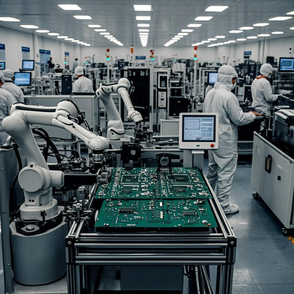
Founded in 2008, Topfast is a leading manufacturer of circuit board design, manufacturing, and assembly with 17 years of experience. As a one-stop PCB solutions provider, we specialize in serving customers with rapid prototyping and small-batch manufacturing needs. We are equipped with state-of-the-art production facilities.