Conductive carbon ink is added to a finished PCB in order to provide a robust and long-lasting electrical interface with another mechanical component, such as a key or dial. It does that in two main ways: it raises the shallow copper contact above the surface of the PCB; and, it protects the PCB contact from oxidation, contaminants, and debris.
Carbon ink also has a defined resistance per area so it is a way to create ‘printed resistors’, particularly ones of non-standard shapes and sizes that can be used with dials and other mechanical interfaces. Conductive carbon ink is hardened by ‘baking’ and will maintain its properties (resistance, shape, conductivity) after the reflow of the PCB during assembly.
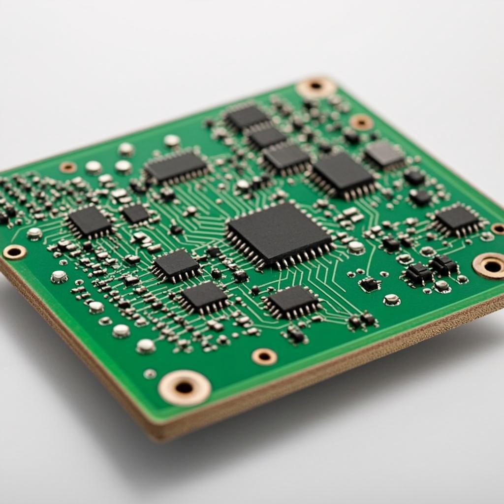
Figure 1 & 2: Examples of carbon contacts applied onto a finished board.
We apply conductive carbon ink using screen-printing, following this process:
Figure 3 & 4: Cross section of PCBs that have had carbon ink applied to copper pads with soldermask overlap.
The datasheets for the carbon-conductive ink is available on our Downloads page; they specify all the properties of the ink that could be relevant to an application (such as resistance per area, etc.) Our design guidelines for defining carbon contacts in your data, and manufacturing tolerances are at PCB Design Guidelines – Carbon Contacts.
Get all the latest news and information about our company, the industry and technology