A Rigid PCB can be Single Sided, Double Sided, or Multilayer. And a rigid PCB is a Solid, inflexible printed circuit Board.
Due to the development trend of aerospace products, including lightweight, miniaturization, multifunction, and assembly densification, a higher requirement has been founded for printed circuit board (PCB) technology and manufacturing process. Rigid PCBs are a kind of circuit board that is fabricated from different substrate materials and have more advantages than ordinarily PCBs.
Furthermore, electromagnetic signals can run quickly and smoothly in rigid PCBs due to the excellent electrical performance and thermal performance of rigid substrate material so rigid PCBs are widely applied in many industries like instruments, automotive, treatment, military, and aerospace. Based on the further development and optimization of rigid PCBs, the subsequent step for them should be Rigid PCBs, Embedded Rigid Circuits, and HDI Flex PCBs, among which Rigid PCBs attracts the foremost attention and applications.
A rigid PCB is a Solid, inflexible printed circuit Board. We all know that a PCB is Single Sided PCB, Double Sided PCB, or Multilayer PCB. At the identical time, a printed circuit board is often Rigid, Flexible, or Rigid-Flex (A combination of Rigid and versatile PCB). So, a Rigid board is a Board that we cannot bend or force out of shape. It’s not flexible. A Rigid PCB can be Single Sided, Double Sided, or Multilayer board.
Once a Rigid printed circuit is manufactured it cannot be modified or folded into the other shape. A rigid circuit card is created of the solid substrate with copper tracks and component layouts where Active and Passive Electronic Components (Through-Hole, SMD Components, or Mixed PCB Assembly) are soldered either by automated Through Hole Soldering Technology like Wave Soldering or Automated Surface Mount Technology (SMT) like Reflow Soldering and Hand Soldering can also be done.
Here are some characteristics of Rigid PCB:
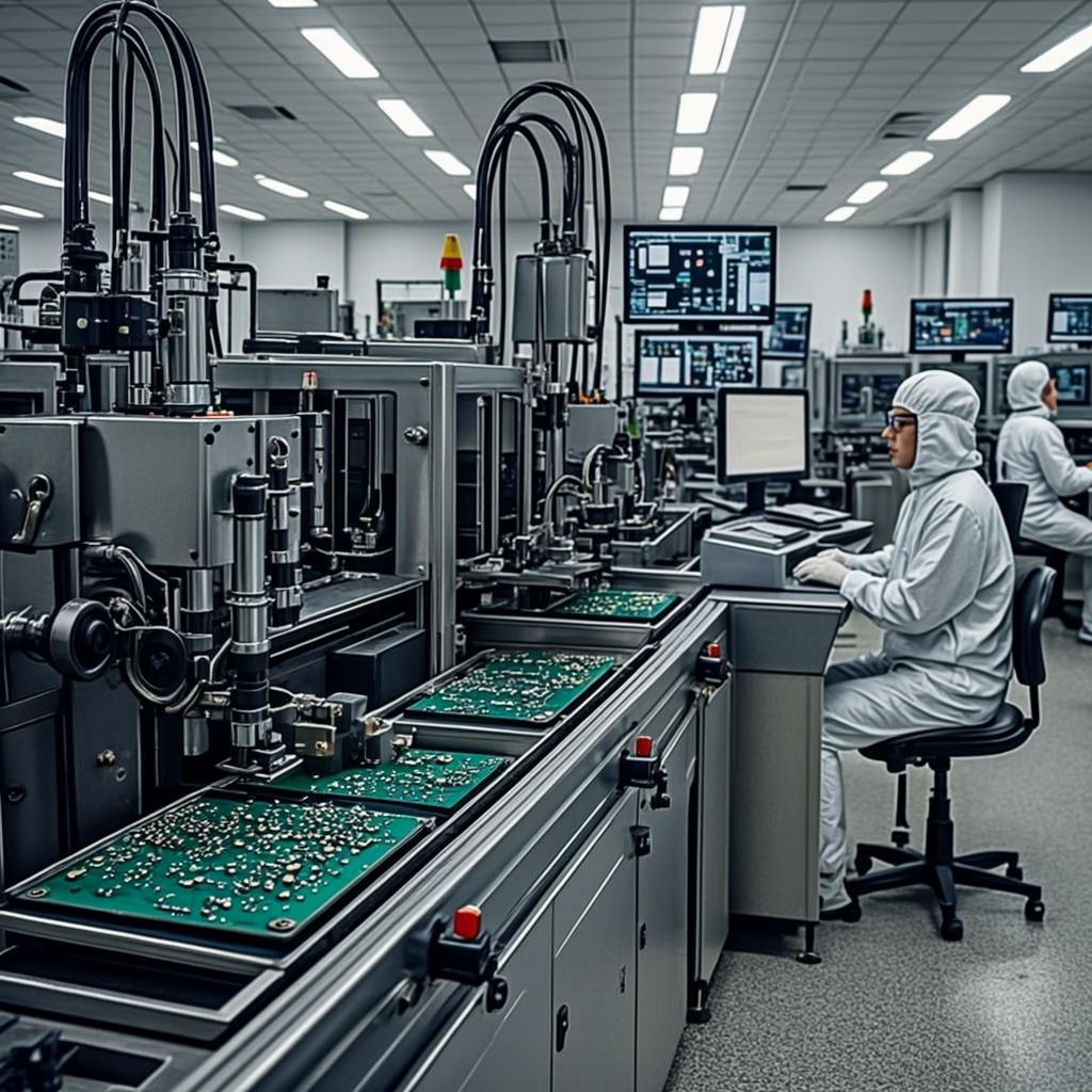
Like any other PCB, rigid PCBs are manufactured by following a certain process. Here, we will discuss each phase in the whole manufacturing process of a Rigid printed circuit board.
Step 1: Material Preparation
The method begins with the bare production boards. These are cleaned using chemicals before they're sent for the application of photoresist film. Generally, an automatic conveyor line is employed to move multiple pieces. The intention of this is often to make sure that the boards don't get damaged in any way. It's also performed to confirm a quick manufacturing process.
Step 2: Exposure of Circuit Pattern
Once the panels have undergone the appliance of the photoresist, the board is then laid with the assorted circuit artwork patterns. This process is performed by exposing the board to UV light, to assist transfer the circuit images onto the assembly panels. This process may be performed on a single or either side of the board.
Step 3: Etching
With the circuit pattern having been transferred onto the board, the subsequent step is etching. this is often where circuit patterns are chemically etched onto the board. This process is performed by specialized handling equipment and automatic chemical etching machines.
Step 4: Drilling
Once the circuit pattern has been etched onto the board, the following step is to drill the holes for the circuit patterns. It's important that the drilled holes are of a specific size, adhering to exact specifications. Generally, PCB manufacturers utilize two kinds of equipment to perform this process. Specialized drilling machines with several drill mechanisms are accustomed create holes in multiple boards. They also utilize laser drills to urge clean, precise holes in an exceedingly very short period of your time.
Step 5: Copper Plating
With the drilling complete, the board can now undergo the copper plating process. this is often where additional copper is applied to the printed circuit to form layer-to-layer interconnections. For this purpose, manufacturers utilize automated copper plating systems. They apply the copper onto the plated through holes.
Step 6: Coverlay Application
For cover and performance purposes, the PCB is roofed with a Coverlay laminate. Polyimide Coverlays are one of the popular options for rigid PCBs. This process comprises aligning and tacking the laminates into place. This process is often performed by hand, or with automated machines.
Step 7: Coverlay Lamination
With the Coverlay aligned and tacked, it now must be laminated to the board. The boards are placed in specialized lamination machines. These machines apply a mix of vacuum, heat, and pressure. This ensures that the laminated is correctly stuck to the board.
Step 8: Stiffener Application
This is often an optional step performed by PCB manufacturers. However, most designs do use this component. Stiffeners are supportive components that are accustomed to preventing the lamination to forestall it from moving, or becoming loose. Generally, stiffeners are applied before the Coverlay lamination process. They're adhered to the board using heat, vacuum, or pressure.
Step 9: Mounting
Once all the components and lamination have been completed, the PCB must be assembled. Generally, Plated Through Hole (PTH) mounting technology is employed for rigid PCBs. During this process, the leads of the components are more mature than the drilled holes. The leads are then soldered to pads on the other side of the board.
Step 10: Testing
For a PCB to be considered acceptable an application, it's to fulfill the wants of the subsequent testing procedures – electrical, AOI, and functional. Electrical testing involves using flying probe test machines to make sure that every one of the electrical connections like shorts, opens, and capacitance, of the PCB, are working properly. Automated Optical Inspection (AOI) involves using an optical imaging system to test the PCB for faults, and soldering and assembly defects. Functional testing is the final step. The functional test machine verifies that the PCB’s hardware is freed from any defects.
These are the fundamental steps utilized in the assembly of rigid PCBs. These PCBs are often constructed with single, double, and multiple layers. For a PCB to satisfy all requirements of the application, it’s important to produce detailed information about the appliance to the PCB manufacturer. This can allow him to style the PCB in step with your needs.
Rigid PCB contains different layers that are joined together using adhesive and warmness, providing a stable form to board material. Following layers are used to develop a rigid PCB.
The substrate layer, also referred base material, is formed of fiberglass. The FR4 is especially used as a substrate material, the foremost common fiberglass that has rigidity and stiffness to the board. Phenolics and epoxies are used as a base material, but they're not pretty much as good as FR4. However, they're less costly and have a novel lousy smell. The decomposition temperature of phenolics is simply too low, leading to delamination of the layer if solder is placed for an extended time.
On the highest of the substrate layer, a copper foil is laminated on the board with the assistance of the added amount of warmth and adhesive. In everyday use, each side of the board is laminated with copper; however, some cheap electronics include just one layer of copper material on the board. Different boards include different thicknesses, which are described in ounces per sq ft.
Solder Mask Layer houses above the copper layer. This layer is added to the board to feature insulation on the copper layer to avoid any damage if any conduction material is touched by the copper layer.
The silkscreen layer is found above the solder mask layer. It's wont to add characters or symbols on the board to grasp the board better. White color is especially used for silkscreen. However, other colors also are available, including grey, red, black, and yellow.
Rigid printed circuit boards offer increased circuit density and might reduce the size and overall weight of the board. This is why JHYPCB use these boards in their several electronic devices and gadgets:
What are the types of rigid PCBs?
Rigid PCB can be divided into single-sided rigid PCB, double-sided rigid PCB, and multi-layer rigid PCB according to the number of layers.
What are the PCB design software?
Well-known PCB design software (computer-aided design, CAD) includes OrCAD, Pads (PowerPCB), Altium Designer, FreePCB, CAM350, etc.
Can you manufacture flexible PCBs?
Absolutely. We can provide flexible PCB manufacturing services for up to 10 layers.
Learn more about our flexible PCB capabilities.
Rigid PCB vs. Flexible PCB: Which is Better?
Both rigid and flexible PCBs have their own advantages. The choice of rigid or flexible PCB depends on cost and application needs.
What are the substrates for rigid PCB manufacturing?
Materials used to manufacture printed circuit boards must have good heat dissipation and insulation properties. A commonly used rigid PCB material is FR-4. JHYPCB provides FR-4, High Tg, Shengyi, Rogers, Arlon, Halogen Free, IT180, Isola, etc.